
Semiconductor Package Assembly Systems and Methods using DAM and Trench Structures

Active Publication Date: 2011-05-19
QUALCOMM INC
View PDF22 Cites 42 Cited by
  • Summary
  • Abstract
  • Description
  • Claims
  • Application Information

AI Technical Summary

Benefits of technology

[0004]According to one embodiment, a packaging system for preventing underfill overflow comprises a package substrate having a solder mask and a die attach site, a solder mask dam on the solder

Problems solved by technology

It is not desirable for underfill to flow onto some parts of the package substrate.
For example, when underfill flows onto an exposed electrical contact pad, such as a bond finger pad, it can prevent electrical contact with the pad or cause mechanical problems.

Method used


Image

  • Semiconductor Package Assembly Systems and Methods using DAM and Trench Structures
  • Semiconductor Package Assembly Systems and Methods using DAM and Trench Structures
  • Semiconductor Package Assembly Systems and Methods using DAM and Trench Structures

Examples


Embodiment Construction

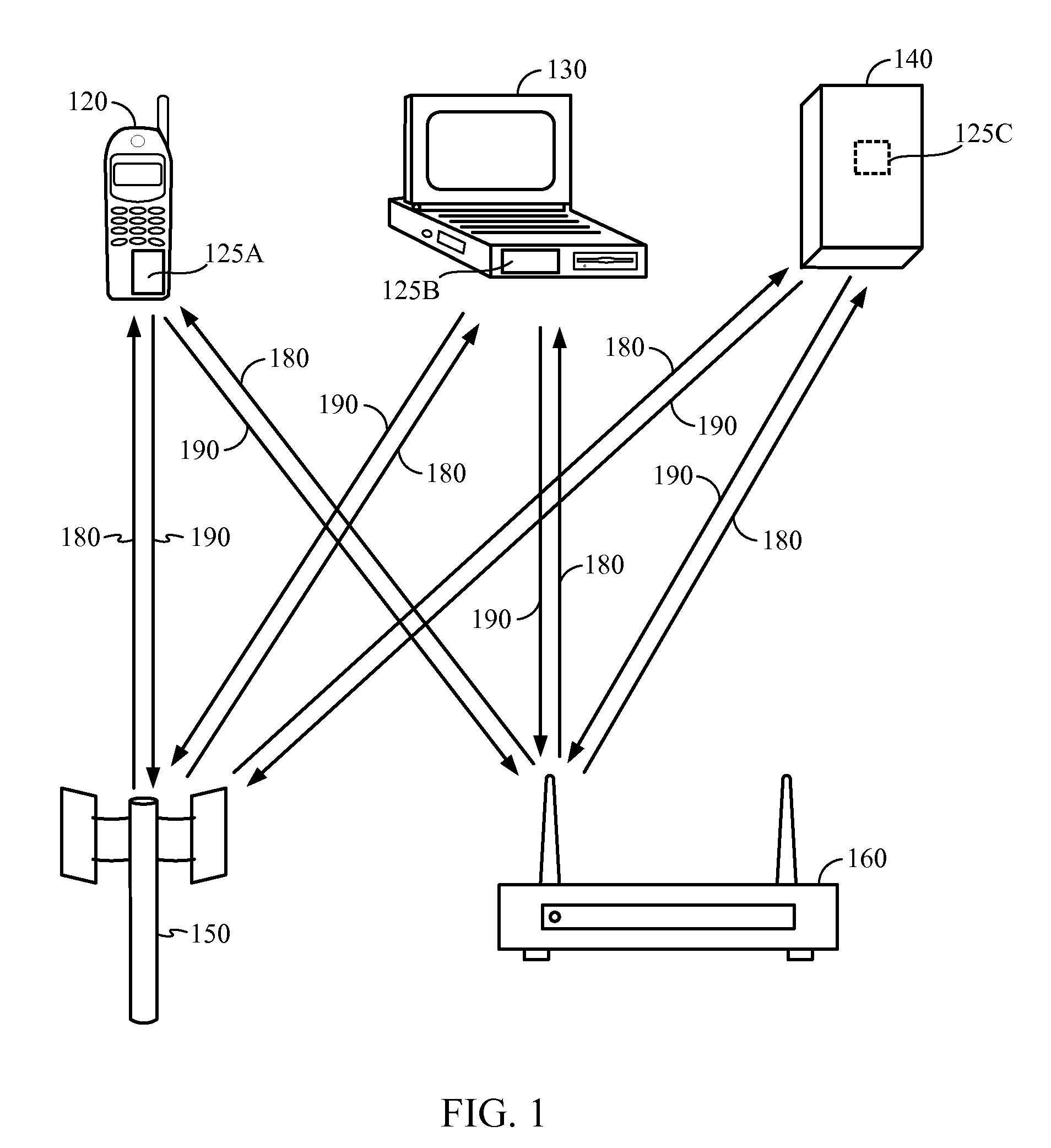
[0017]FIG. 1 shows an exemplary wireless communication system 100 in which an embodiment of the disclosure may be advantageously employed. For purposes of illustration, FIG. 1 shows three remote units 120, 130, and 140 and two base stations 150, 160. It will be recognized that wireless communication systems may have many more remote units and base stations. The remote units 120, 130, and 140 include improved semiconductor chip packages 125A, 125B, and 125C, respectively, such as the semiconductor chip packages discussed in more detail below. FIG. 1 shows the forward link signals 180 from the base stations 150, 160 and the remote units 120, 130, and 140 and the reverse link signals 190 from the remote units 120, 130, and 140 to base stations 150, 160.

[0018]In FIG. 1, the remote unit 120 is shown as a mobile telephone, the remote unit 130 is shown as a portable computer, and the remote unit 140 is shown as a computer in a wireless local loop system. For example, the remote unit 120 ma...


PUM


Abstract

A packaging system for preventing underfill overflow includes a package substrate having a solder mask a die attach site, a solder mask dam on the solder mask proximal to the die attach site, and a trench in the solder mask proximal to the die attach site. The trench and the solder mask dam are adapted to constrain flow of an underfill material.

Description

TECHNICAL FIELD[0001]The present description generally relates to semiconductor chip packaging and, more specifically, to techniques using a dam and a trench to control flow of underfill.BACKGROUND[0002]Semiconductor chip packages are used in a variety of devices and conventionally include a package substrate and one or more dies mounted on the package substrate. Semiconductor chip packages sometimes include underfill to provide thermal and mechanical support to the die on the package substrate. For instance, in a conventional design using a flip chip ball grid array die, underfill is applied, as a liquid, between the die and the substrate, thereby filling in the spaces within the ball grid array. The underfill then hardens.[0003]It is not desirable for underfill to flow onto some parts of the package substrate. For example, when underfill flows onto an exposed electrical contact pad, such as a bond finger pad, it can prevent electrical contact with the pad or cause mechanical probl...

Claims


Application Information

Patent Timeline
IPC IPC(8): H01L23/28H01L21/56
CPCH01L21/563H01L2224/16225H01L2224/26175H01L2224/32225H01L2224/73204H01L2224/83385H01L2924/15311H01L2924/00012H01L2924/00
Inventor ZANG, RUEY KAEHSU, WEN-SUNG
Owner QUALCOMM INC
Features
  • Generate Ideas
  • Intellectual Property
  • Life Sciences
  • Materials
  • Tech Scout
  • Unparalleled Data Quality
  • Higher Quality Content
  • 60% Fewer Hallucinations
Learn More