Coupled waveguide photo detector

a photo detector and waveguide technology, applied in the field of photo detection, can solve the problems of limiting the performance of many systems that depend on low distortion operation, generating non linear distortion at high optical power, and generating non linear distortion for typical photo detectors

Inactive Publication Date: 2011-05-19
RGT UNIV OF CALIFORNIA
View PDF7 Cites 18 Cited by
  • Summary
  • Abstract
  • Description
  • Claims
  • Application Information

AI Technical Summary

Benefits of technology

[0012]An embodiment of the invention provides a coupled waveguide photo detector device. Optically, the device includes an input waveguide. An output waveguide is coupled to the input waveguide with a nonuniform coupling coefficient in a coupling section. An absorber is included in the coupling section to convert an absorbed portion of optical radiation into photo current. The location of absorber and the optical radiation intensity pattern in the

Problems solved by technology

However, typical photo detectors saturate and generate more non linear distortion at high optical powers.
This limits the performance of many systems that depend upon low distortion operation.
However, the nonlinearity increases significantly at high optical power for all photo detectors

Method used


Image

  • Coupled waveguide photo detector
  • Coupled waveguide photo detector
  • Coupled waveguide photo detector

Examples


Embodiment Construction

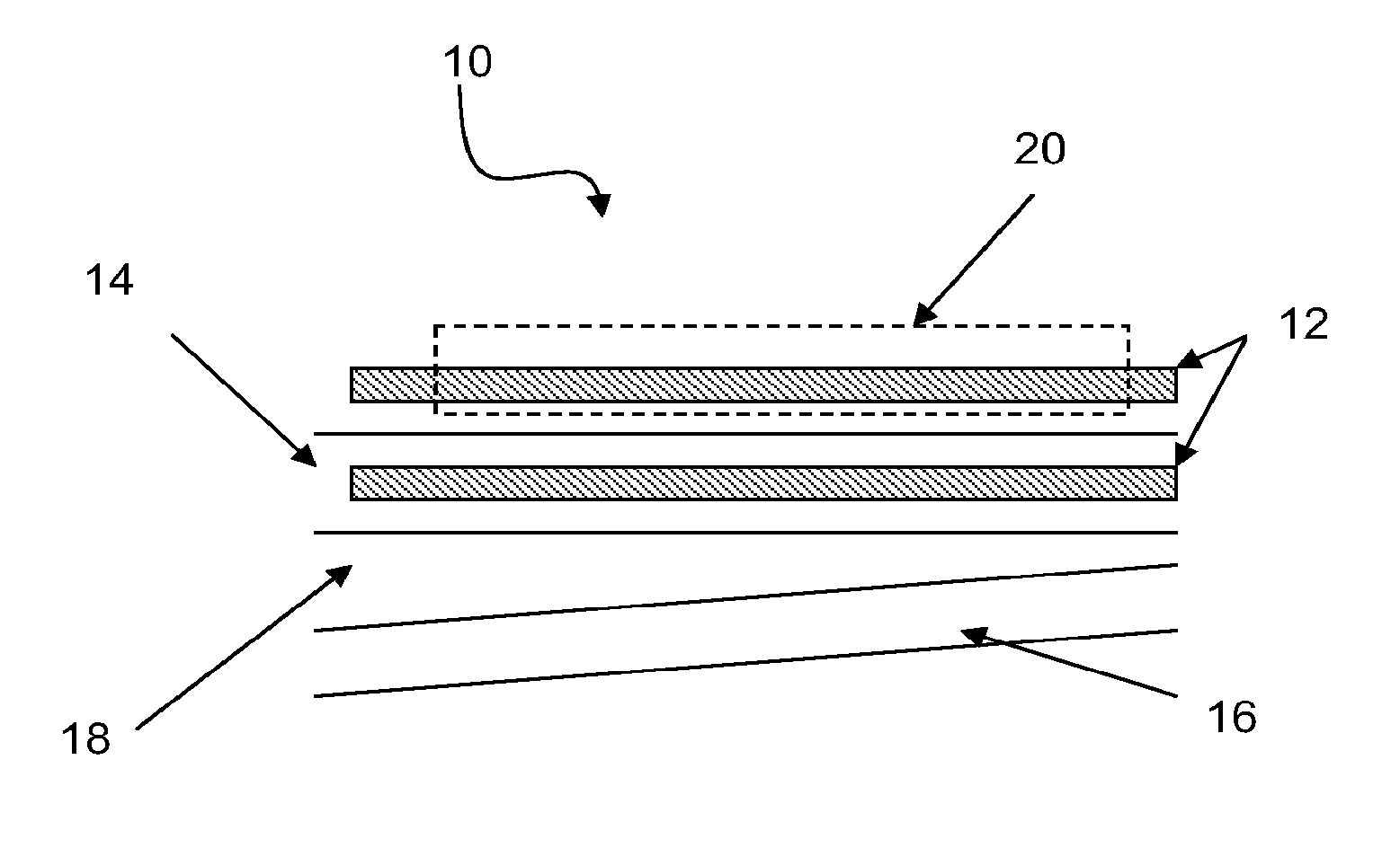
[0020]In a waveguide photo detector of the invention, currents are induced in an electrical transmission line. To achieve in-phase addition of electrical currents collected from different photo detectors or different parts of the extended photo detector structure while the optical wave propagates, the currents induced in the coupling section in different parts of the extended detector or a series of detectors are transmitted via an electrical transmission line which is velocity matched to the optical waveguide.

[0021]An embodiment of the invention provides a directional coupled waveguide photo detector device. The device includes an input waveguide. An output waveguide is optically coupled to the input waveguide through a coupling section. Coupling is achieved in the coupling section with two coupled waveguides (portions of the input and output waveguides similar to a directional coupler) or a multimode interference coupler. The coupling section preferably has a nonuniform coupling c...


PUM


Abstract

An embodiment of the invention provides a coupled waveguide photo detector device. Optically, the device includes an input waveguide. An output waveguide is coupled to the input waveguide with a nonuniform coupling coefficient in a coupling section. An absorber is included in the coupling section to convert an absorbed portion of optical radiation into photo current. The location of absorber and the optical radiation intensity pattern in the coupling section are set to control the maximum intensity of output power absorbed by the output waveguide to be within a predetermined limit that avoids saturation. The absorber is also part of a transmission line collector which has a phase and group velocity to match those of the optical wave in the coupling section such that currents collected by the transmission line collector add in phase as the optical wave propagates in the output waveguide.

Description

PRIORITY CLAIM AND REFERENCE TO RELATED APPLICATION[0001]Priority is claimed pursuant to 35 U.S.C. §119 and all applicable statutes and treaties from prior U.S. provisional application Ser. No. 61 / 127,302, filed on May 12, 2008.STATEMENT OF GOVERNMENT INTEREST[0002]This invention was made with government support under contract No. N66001-02-2-8938 TDL 46 awarded by Defense Advanced Research Projects Agency (DARPA) via the Space and Naval Warfare Systems (SPAWAR). The government has certain rights in the invention.FIELD[0003]A field of the invention is photo detection. An example application of the invention is high power, large bandwidth photo detection. A particular preferred application of the invention is in digital and analog fiber optic communication systems. Another preferred application of the invention is to solar panels.BACKGROUND[0004]Photo detectors convert radiation into electrical energy. Their operation is critical to many mixed signal environments, e.g., optoelectroni...

Claims


Application Information

Patent Timeline
IPC IPC(8): G02B6/26G02B6/42
CPCG02B6/12004G02B2006/12195G02B2006/12147G02B6/125
Inventor CHANG, WILLIAM S.C.YU, PAUL KIT LAI
Owner RGT UNIV OF CALIFORNIA
Why Eureka
Try Eureka