Multi-Layer Reconfigurable Switches

Inactive Publication Date: 2011-05-26
HEWLETT-PACKARD ENTERPRISE DEV LP
View PDF5 Cites 35 Cited by
  • Summary
  • Abstract
  • Description
  • Claims
  • Application Information

AI Technical Summary

Problems solved by technology

However, the design and manufacture of nanoscale electronic devices present many new problems need to be addressed before large-scale commercial production of nanoscale electronic devices and incorporation of nanoscale electronic devices into microscale and larger-scale systems, devices, and products.

Method used


Image

  • Multi-Layer Reconfigurable Switches
  • Multi-Layer Reconfigurable Switches
  • Multi-Layer Reconfigurable Switches

Examples


Embodiment Construction

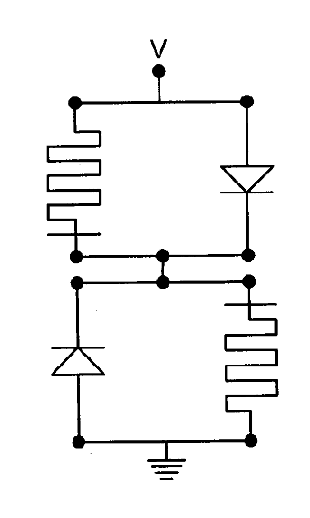
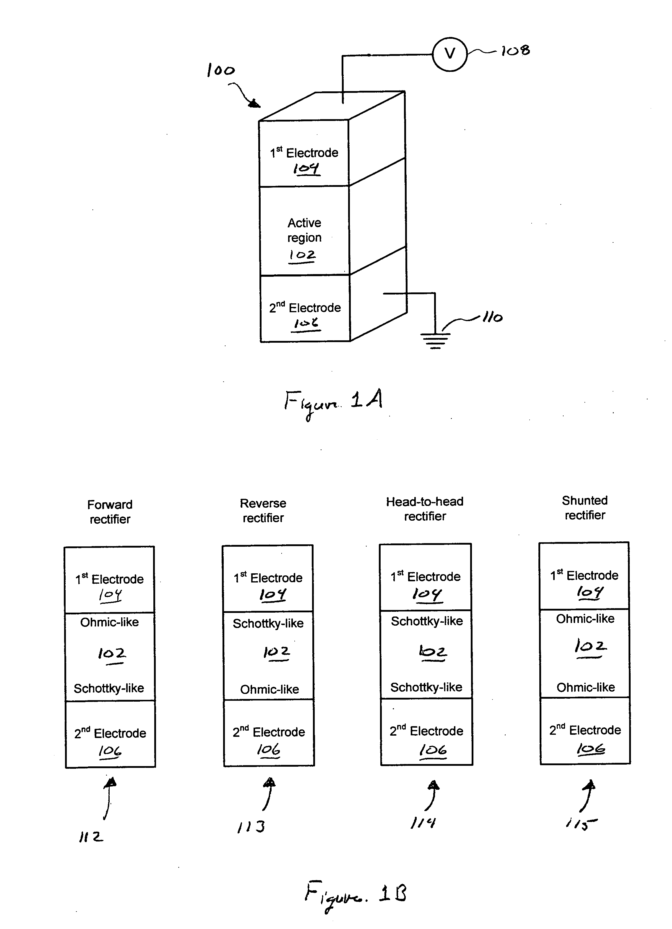
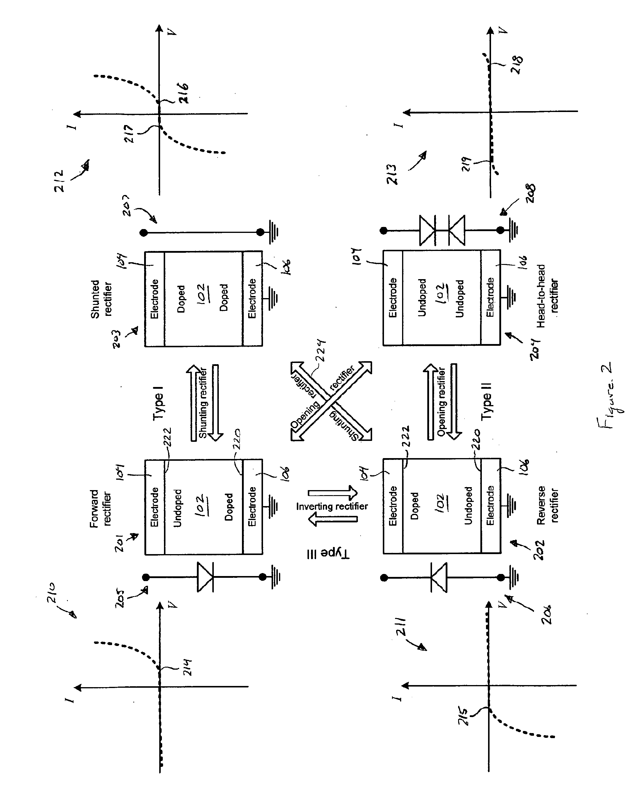
[0016]Various embodiments of the present invention are directed to nanoscale, two-terminal, electronic switches, which are nonvolatile and combine reconfigurable diode rectifying states with memristive switching. A switch configured in accordance with embodiments of the present invention is composed of an active region sandwiched between two electrodes. The two interfaces between the active region and the electrodes are Schottky contacts. The active region is a diode that can be switched into one of four different rectifying states by applying an electrical field of an appropriate magnitude and polarity across the active region. The electric field changes the Schottky contacts at the interfaces to have Ohmic-like barriers and / or Schottky-like barriers, thus enabling the active region to be configured and the switch to operate as one of the four types of rectifiers: a forward rectifier, a reverse rectifier, a shunted rectifier, and a head-to-head rectifier. The active region remains ...


PUM


Abstract

Embodiments of the present invention are directed to reconfigurable two-terminal electronic switch devices (100) comprising a compound (102) sandwiched between two electrodes (104,106). These devices are configured so that the two electrode / compound interface regions can be either rectifying or conductive, depending on the concentration of dopants at the respective interface, which provides four different device operating characteristics. By forcing charged dopants into or out of the interface regions with an applied electric field pulse, a circuit element can be switched from one type of stable operation to another in at least three different ways. A family of devices built to express these properties display behaviors that provide new opportunities for nanoscale electronic devices.

Description

TECHNICAL FIELD[0001]Embodiments of the present invention are related to nanoscale electronic devices, and, in particular, to re-configurable diode switches that can be implemented in crossbar arrays.BACKGROUND[0002]Significant research and development efforts are currently directed towards designing and manufacturing nanoscale electronic devices, such as nanoscale memories. Nanoscale electronics promise a number of advantages over microscale, photolithography-based electronics, including significantly reduced features sizes and the potential for self-assembly and for other relatively inexpensive, non-photolithography-based fabrication methods. However, the design and manufacture of nanoscale electronic devices present many new problems need to be addressed before large-scale commercial production of nanoscale electronic devices and incorporation of nanoscale electronic devices into microscale and larger-scale systems, devices, and products.[0003]Studies of switching in nanometer-sc...

Claims


Application Information

Patent Timeline
Patent Type & Authority Applications(United States)
IPC IPC(8): H01L29/86B82Y99/00
CPCH01L27/101H01L27/1021H01L29/861H01L29/8615H01L29/8616H01L45/147H01L45/08H01L45/1233H01L45/14H01L45/145H01L45/146H01L29/872H10N70/24H10N70/881H10N70/883H10N70/8836H10N70/826H10N70/8833H01L29/41
Inventor YANG, JIANHUABORGHETTI, JULIENSTEWART, DUNCANWILLIAMS, R. STANLEY
Owner HEWLETT-PACKARD ENTERPRISE DEV LP
Why Eureka
Try Eureka