Clock hand-off circuit

Active Publication Date: 2011-06-02
ADVANTEST CORP
8 Cites 46 Cited by

AI-Extracted Technical Summary

Problems solved by technology

However, the logic circuit 12 has a problem of a large amount of switching noise.
Such switching noise has an effect on the high-precision circuit 14, resulting in degraded timing precision.
Furthermore, the phase relation between these clocks fluctuates due to irregularities in the process or the like.
Accordingly, in a case in which a high-speed clock is employed, such fluctuation in the phase relation approaches the period of the clock, leading to a problem in that such an arrangement does not...

Method used

[0070]As the phase of the third clock CK3 advances, the count value COUNT becomes larger. Conversely, as the phase of the third clock CK3 is delayed, the count value COUNT becomes smaller. Thus, by selecting the phase of the third clock CK3 such that the count value COUNT is within a predetermined range, such an arrangement is capable of optimizing the edge timing of the third cloc...

Benefits of technology

[0012]The present invention has been made in order to solve such a problem. Accordingly, it is a general purpose of t...

Abstract

A second latch latches the output data of a first latch using a third clock having the same frequency as that of a first clock. A third latch latches the output data of the second latch using a second clock having a frequency N (N represents an integer) times that of the first clock and the third clock. The second clock and the third clock have a frequency division/multiplication relation therebetween.

Application Domain

Technology Topic

Image

  • Clock hand-off circuit
  • Clock hand-off circuit
  • Clock hand-off circuit

Examples

  • Experimental program(1)

Example

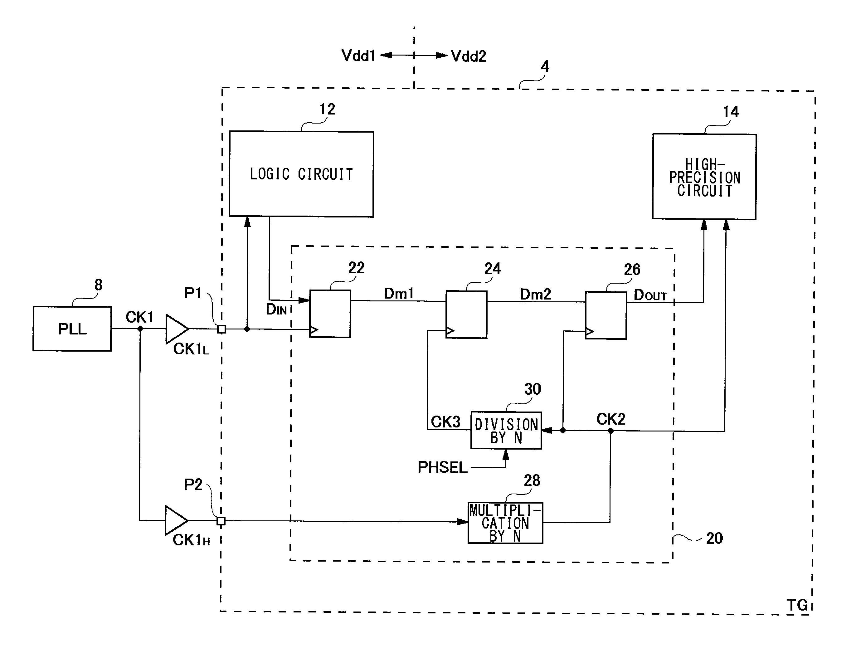
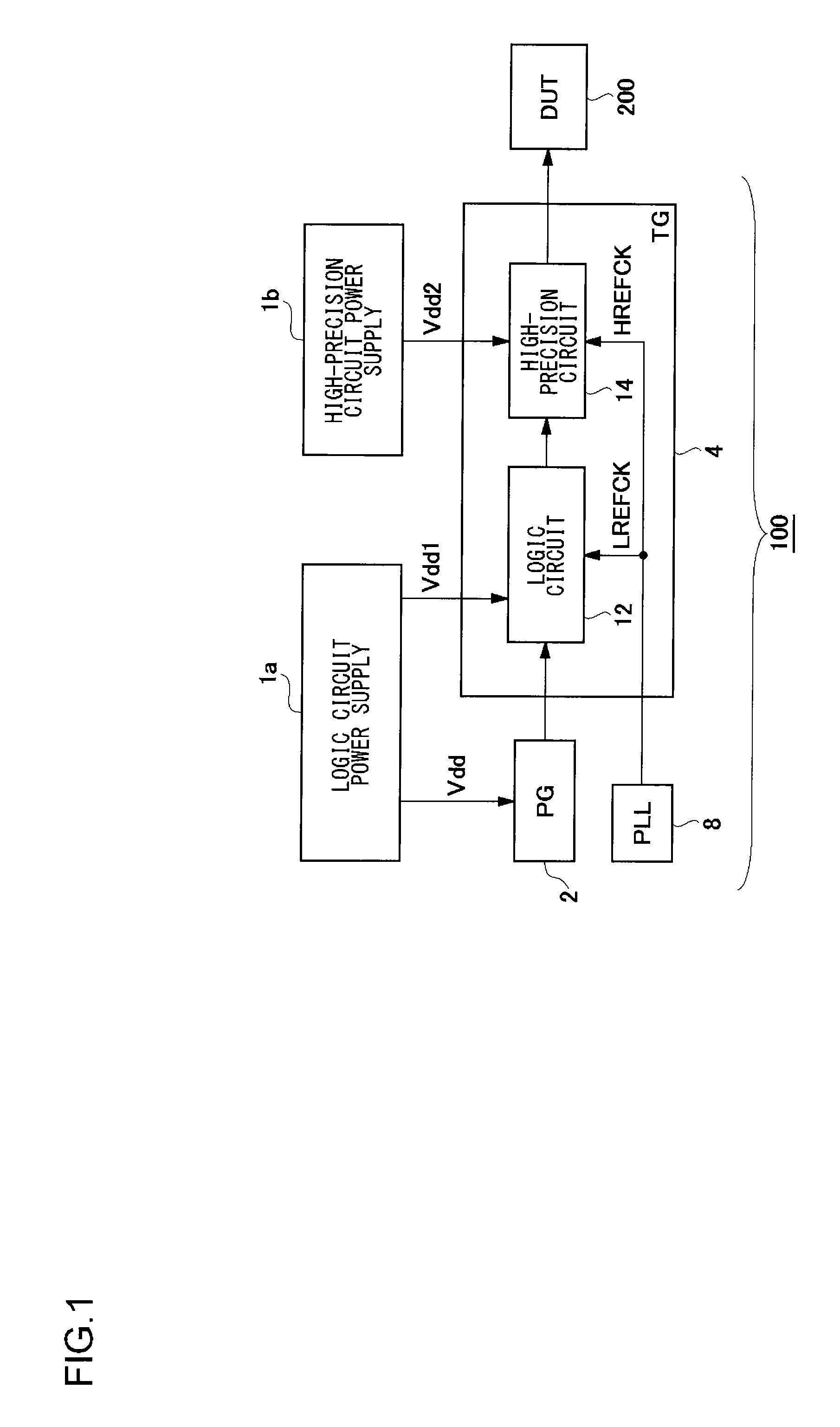
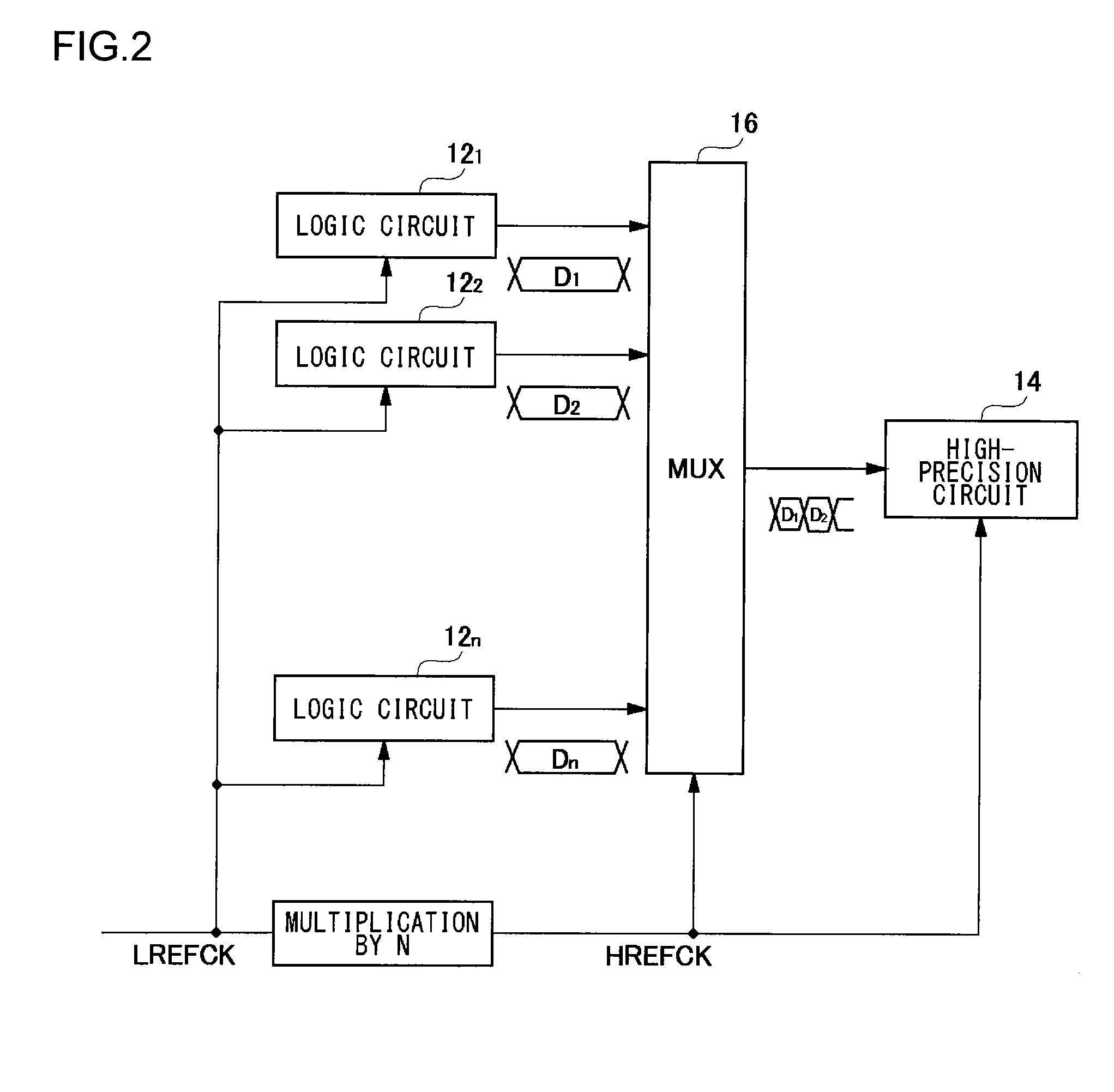
[0045]Description will be made below regarding preferred embodiments according to the present invention with reference to the drawings. The same or similar components, members, and processes are denoted by the same reference numerals, and redundant description thereof will be omitted as appropriate. The embodiments have been described for exemplary purposes only, and are by no means intended to restrict the present invention. Also, it is not necessarily essential for the present invention that all the features or a combination thereof be provided as described in the embodiments.
[0046]In the present specification, the state represented by the phrase “the member A is connected to the member B” includes a state in which the member A is indirectly connected to the member B via another member that does not affect the electric connection therebetween, in addition to a state in which the member A is physically and directly connected to the member B. Similarly, the state represented by the phrase “the member C is provided between the member A and the member B” includes a state in which the member A is indirectly connected to the member C, or the member B is indirectly connected to the member C via another member that does not affect the electric connection therebetween, in addition to a state in which the member A is directly connected to the member C, or the member B is directly connected to the member C.
[0047]FIG. 3 is a circuit diagram which shows a configuration of a timing generator 4 mounting a clock hand-off circuit 20 according to an embodiment. The timing generator 4 includes a logic circuit 12, a high-precision circuit 14, and a clock hand-off circuit 20, which are monolithically integrated on a single semiconductor substrate. As described above with reference to FIG. 1, the logic circuit 12 and the high-precision circuit 14 operate while receiving different respective power supply voltages Vdd1 and Vdd2. A clock generator 8 is configured as a PLL circuit, for example, and outputs a first clock CK1 at a first frequency f1. The timing generator 4 receives the clock to be used by the logic circuit 12 and the clock to be used on the high-precision circuit 14 side via separate clock terminals P1 and P2, respectively. The first clock CK1 is divided into one clock CLK1L that is supplied to the logic circuit 12 via a clock terminal P1, and another clock CLK1H that is supplied to the high-precision circuit 14 via a clock terminal P2.
[0048]The logic circuit 12 generates input data DIN in synchronization with the first clock CK1L having a first frequency f1 output from the clock generator 8. The clock hand-off circuit 20 hands off the input data DIN that is in synchronization with the first clock CLK1L to the second clock CK2, which has a second frequency f2, which is N times the first frequency f1. The high-precision circuit 14 receives the output data DOUT output from the clock hand-off circuit 20, and operates in synchronization with the second clock CK2. Description will be made regarding an arrangement in which N=8 for simplicity of description. However, N can be determined as desired, and is not restricted in particular.
[0049]The above is the overall configuration of the timing generator 4. Next, description will be made regarding the clock hand-off circuit 20.
[0050]The clock hand-off circuit 20 includes a first latch 22, a second latch 24, a third latch 26, a frequency multiplying circuit 28, and a frequency dividing circuit 30.
[0051]The first latch 22 latches the input data DIN using the first clock CK1L. The second latch 24 latches the output data (first intermediate data Dm1) of the first latch 22 using a third clock CK3 having the same frequency as that of the first clock CK1L.
[0052]The third latch 26 latches the output data (second intermediate data Dm2) of the second latch 24 using the second clock CK2 having the frequency f2, which is N times (N represents an integer) the frequency of the first clock CK1 and the third clock CK3.
[0053]There is a reciprocal frequency division/multiplication relation between the second clock CK2 and the third clock CK3. For example, the second clock CK2 may be generated by multiplying the third clock CK3 by N. Conversely, the third clock CK3 may be generated by dividing the second clock CK2 by N. In the present embodiment, the latter method is employed.
[0054]The input data DIN is handed off from the clock CK1L to the clock CK2 via two steps, i.e., a step from the first clock CK1L to the third clock CK3, and a step from the third clock CK3 to the second clock CK2. An essentially synchronous phase relation is maintained between the second clock CK2 and the third clock CK3, which have a frequency division/multiplication relation. Thus, with the clock hand-off circuit 20 shown in FIG. 3, the downstream components of the second latch 24 operate in synchronization with each other as long as the phase difference between the first clock CK1L and the third clock CK3 satisfies a predetermined relation. Thus, such an arrangement hands off data from one clock to another clock in a sure manner.
[0055]Next, description will be made regarding the relation between the clocks shown in FIG. 3.
[0056]The frequency dividing circuit 30 divides, by N, the second clock CK2 having the second frequency f2, which is N times the frequency of the first clock CK1, thereby generating the third clock CK3. The frequency multiplying circuit 28 multiplies the first clock CK1H by N, thereby generating the second clock CK2.
[0057]The above is the configuration of the clock hand-off circuit 20. FIG. 4 is a time chart which shows the operation of the clock hand-off circuit 20 shown in FIG. 3.
[0058]Instead of using the first clock CK1H without change as the third clock CK3, by generating the third clock CK3 by dividing the frequency of the second clock CK2, such an arrangement is capable of adjusting the phase of the third clock CK3 in increments of the period of the second clock CK2 (1/f2). This is why such an arrangement in which the frequency of the second clock CK2 is divided by N is capable of selecting one of N phases φ0 through φ7. Of the third clocks CK3 (φ0 to φ7) having eight respective phases each obtained by dividing the frequency of the second clock CK2 shown in FIG. 4 by 8, one clock is selected according to a phase selection signal PHSEL (=0 to 7), and the third clock CK3 thus selected is supplied to the second latch 24.
[0059]Next, description will be made regarding an optimization method for optimizing the phase of the third clock CK3 and a circuit configuration for implementing the optimization method.
[0060]FIG. 5 is a circuit diagram which shows a configuration of a phase adjustment circuit 40 configured to control the phase φ of the third clock CK3. The phase adjustment circuit 40 includes a counter 42, an AND gate 44, and an AND gate 46.
[0061]The counter 42 counts, using the second clock CK2, the time difference between the edge timing of the third clock CK3 and the edge timing of the first intermediate data Dm1 received from the first latch 22. The counter 42 may measure the time difference between a positive edge of the first intermediate data Dm1 and an edge of the third clock CK3. Also, the counter 42 may measure the time difference between a negative edge of the first intermediate data Dm1 and an edge of the third clock CK3. The phase adjustment circuit 40 shown in FIG. 5 is configured so as to optimize the phase of the third clock CK3 based upon the latter method.
[0062]The AND gate 44 masks the second clock CK2 using the first intermediate data Dm1. The clock CK4 thus masked is supplied to the counter 42. The counter 42 counts the clock CK4 thus received.
[0063]The AND gate 46 generates the logical AND of the second intermediate data Dm2 received from the second latch 24 and the inversion of the output data DOUT. The count value COUNT held by the counter 42 is initialized according to a clear signal CLR output from the AND gate 46.
[0064]FIG. 6 is a time chart which shows the operation of the phase adjustment circuit 40 shown in FIG. 5. In a step in which the phase is adjusted, a predetermined pattern is input as the input data DIN. In the time chart shown in FIG. 6, the input data DIN is shown as a pattern in which the level is switched in the order low level, high level, low level. The first intermediate data Dm1 output from the first latch 22 is switched in the order low level, high level, low level, according to the input data DIN.
[0065]When the first intermediate data Dm1 is switched to high level at the time point t1, the AND gate 44 releases the second clock CK2 from being cut off, and accordingly, the second clock CK2 is output to the counter 42. In this stage, the counter 42 starts the count operation.
[0066]With the i-th phase (0≦i 3, the first intermediate data Dm1 is latched at a positive edge of the i-th phase clock thus selected, thereby generating the second intermediate data Dm2. When the second intermediate data Dm2 is switched to high level at the time point t2, the clear signal CLR output from the AND gate 46 is asserted, thereby resetting to zero the count value of the counter 42. Subsequently, the count value of the counter 42 is counted up in increments of 1 per pulse. It should be noted that the counter 42 has a period (dead band DB) in which the counter cannot provide an effective count operation immediately after the clear operation. Accordingly, a certain number of pulses are not counted immediately after the clear operation. In the time chart shown in FIG. 6, the dead band τd occurs for a period of two clocks.
[0067]At the time point t3, the first intermediate data Dm1 is switched to low level according to the transition of the input data DIN. In this state, the AND gate 44 cuts off the second clock CK2, and accordingly, the clock CK4 is not supplied to the counter 42, thereby stopping the counting operation of the counter 42. The counter 42 holds the count value COUNT until the clear signal CLR is asserted when new input data DIN is supplied. That is to say, with such an arrangement, the count value COUNT is held regardless of the states of the first clock CK1L and CK1H. Thus, such an arrangement has the advantage that there is no need to stop these clocks in a step for optimizing the phase.
[0068]The resulting count value COUNT of the counter 42 represents a value that corresponds to a period of time t from an edge timing (t2) of the third clock CK3 until a timing (t3) of a negative edge of the first intermediate data Dm1. The period of time τ is represented by the following Expression using the period T2 (=1/f2) of the second clock CK2.
τ=τd+COUNT×T2
[0069]In a case in which the dead band of the counter 42 is negligibly small, the count value COUNT is represented by the Expression τ=COUNT×T2.
[0070]As the phase of the third clock CK3 advances, the count value COUNT becomes larger. Conversely, as the phase of the third clock CK3 is delayed, the count value COUNT becomes smaller. Thus, by selecting the phase of the third clock CK3 such that the count value COUNT is within a predetermined range, such an arrangement is capable of optimizing the edge timing of the third clock CK3 so as to satisfy the set-up conditions and the hold conditions with respect to the second latch 24, and specifically by optimizing the edge timing of the third clock CK3 to be in the vicinity of the center of the unit interval of the first intermediate data Dm1. In the time chart shown in FIG. 6, the optimal edge timing corresponds to when the count value COUNT is from 2 to 4.
[0071]The operation for optimizing the phase of the third clock CK3 can be executed according to the following procedure.
[0072]First Procedure
[0073]FIG. 7 is a flow chart which shows the first procedure for performing phase optimization by means of the phase adjustment circuit 40.
[0074]In the optimization operation, the following steps are executed while incrementing the value of the variable PHSEL from 0 to 7 in increments of 1 (S100).
[0075]The variable PHSEL is set to i (0≦i 3 to φi (S102). Subsequently, a predetermined pattern is applied as the input data DIN (S103), following which the count value of the counter 42 is read out (S104). When the count value COUNT is within an optimal range (“YES” in S106), the current variable PHSEL is determined to be optimal (S108), and the optimization operation ends.
[0076]When the count value COUNT is outside the optimal range (“NO” in S106), the variable PHSEL is incremented, the flow returns to Step S102, and the same processing is repeatedly performed.
[0077]With the processing shown in the flow chart in FIG. 7, such an arrangement provides a third clock CK3 having an optimal phase by performing the aforementioned processing at most N times. Furthermore, such an arrangement holds the count value COUNT until a new pattern is input. Accordingly, such an arrangement does not require a control operation for stopping and restarting the reference clock CK1. Thus, such an arrangement does not require a wait time for waiting for the stable state of the circuit, thereby providing a high-speed initializing operation.
[0078]Second Procedure
[0079]FIG. 8 is a flow chart which shows the second procedure for performing the phase optimization by means of the phase adjustment circuit 40.
[0080]First, the value of the variable PHSEL is set to a initial value (=0), thereby setting the phase of the third clock CK3 to φ0 (S200). The initial value INIT is not restricted to 0.
[0081]Subsequently, a predetermined pattern is applied as the input data DIN (S200), following which the count value COUNT of the counter 42 is read out (S204). When the count value COUNT is lower than the upper limit value H (=4) of the optimal range (“NO” in S206), and the count value COUNT is smaller than the lower limit L (=2) of the optimal range (“NO” in S210), the variable PHSEL is set to the initial value, and the optimization operation ends.
[0082]In Step S206, a case in which the count value COUNT is greater than the upper limit H (=4) (“YES” in S206) means that the edge timing of the third clock CK3 is earlier than the optimal edge timing. Thus, in this case, the variable PHSEL is set to a first value X (=2) which differs from the initial value INIT (S208). The first value is set to a value which is greater than the initial value by a predetermined value (e.g., 2). As a result, the timing of the third clock CK3 is shifted backward by a period of two cycles, thereby optimizing the timing of the third clock CK3.
[0083]In Step S120, a case in which the count value COUNT is smaller than the lower limit H (=2) (“YES” in S210) means that the edge timing of the third clock CK3 is later than the optimal edge timing. Accordingly, in order to shift the timing of the third clock CK3 forward, the value of the variable PHSEL is set to a second value Y (=5) that differs from the initial value (S212). As a result, the third clock CK3 is shifted back so as to straddle the current cycle, thereby setting the timing of the third clock CK3 to be earlier than that in the initial state.
[0084]With the second procedure, such an arrangement can optimize the phase of the third clock CK3 by applying a pattern only once.
[0085]Description has been made regarding the present invention with reference to the embodiments. However, the above-described embodiments show only the mechanisms and applications of the present invention for exemplary purposes only, and are by no means intended to be interpreted restrictively. Rather, various modifications and various changes in the layout can be made without departing from the spirit and scope of the present invention defined in appended claims.

PUM

no PUM

Description & Claims & Application Information

We can also present the details of the Description, Claims and Application information to help users get a comprehensive understanding of the technical details of the patent, such as background art, summary of invention, brief description of drawings, description of embodiments, and other original content. On the other hand, users can also determine the specific scope of protection of the technology through the list of claims; as well as understand the changes in the life cycle of the technology with the presentation of the patent timeline. Login to view more.

Similar technology patents

Method and device for forecasting reservoir yield

InactiveCN101906966AHigh precisionSurveyWellheadVolume factor
Owner:PETROCHINA CO LTD

Classification and recommendation of technical efficacy words

Why Eureka
Try Eureka