Flexible Wiring Substrate

a flexible wiring and substrate technology, applied in the direction of printed circuit details, printed circuits, electrical apparatus, etc., can solve the problems of increasing the size of the protruding substrate portion or the area in which the electrode terminals are arranged on the electrical instrument substrate, and the wiring terminals cannot be electrically connected to the corresponding electrode terminals, etc., to achieve convenient insertion, easy insertion, and simplified manufacturing process

Active Publication Date: 2011-06-09
HOSIDEN CORP
View PDF11 Cites 22 Cited by
  • Summary
  • Abstract
  • Description
  • Claims
  • Application Information

AI Technical Summary

Benefits of technology

[0020]According to this aspect, the protruding substrate portion extending to one side edge is configured so as to be foldable toward a direction opposite from the extension direction thereof, whereby the manufacturing process can be simplified by providing a wiring terminal to the same surface of the protrud

Problems solved by technology

Accordingly, a problem is encountered in that these wiring terminals cannot be electrically connected to the corresponding electrode terminals.
However, a disadvantage o

Method used


Image

  • Flexible Wiring Substrate
  • Flexible Wiring Substrate
  • Flexible Wiring Substrate

Examples


embodiment 1

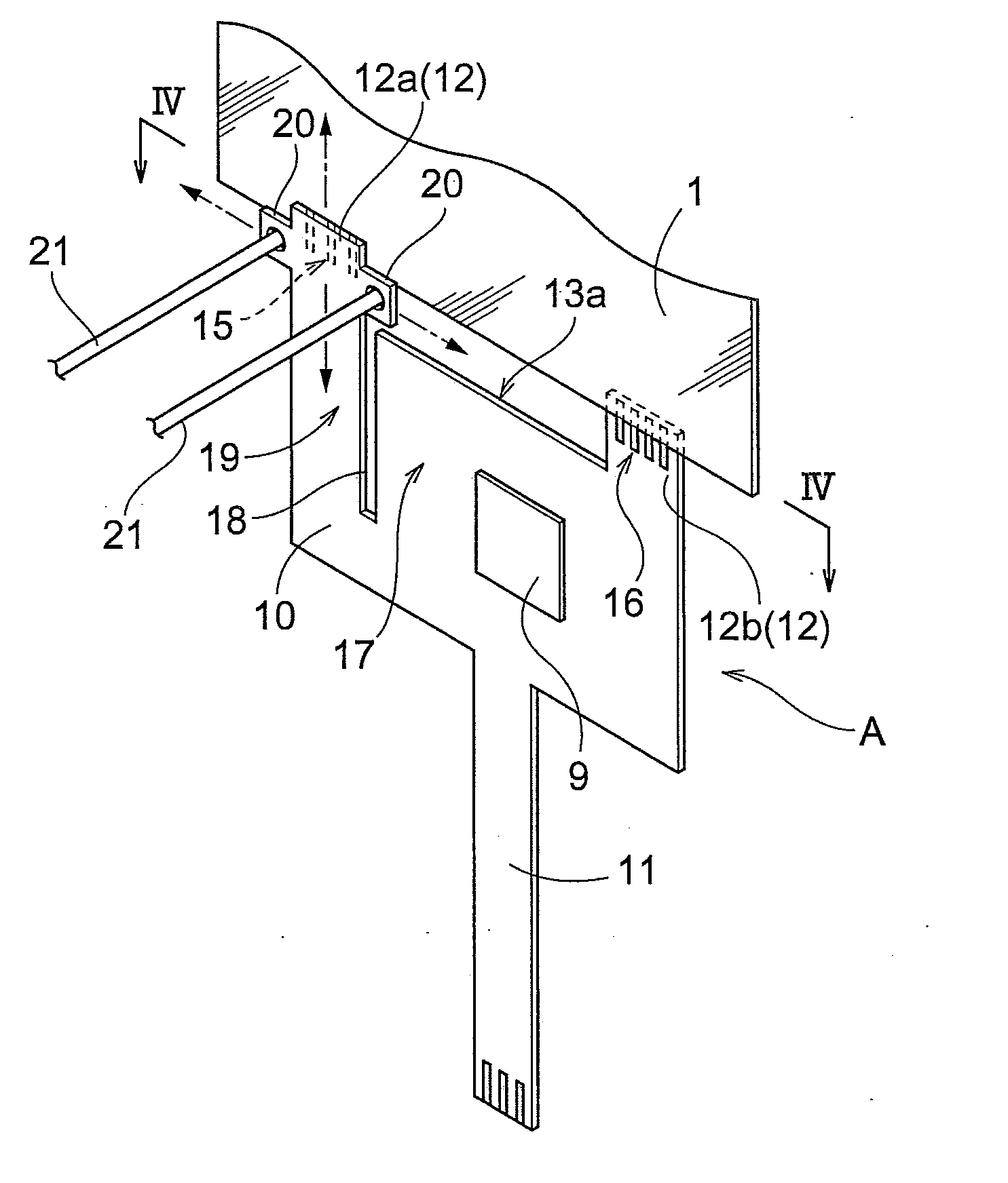
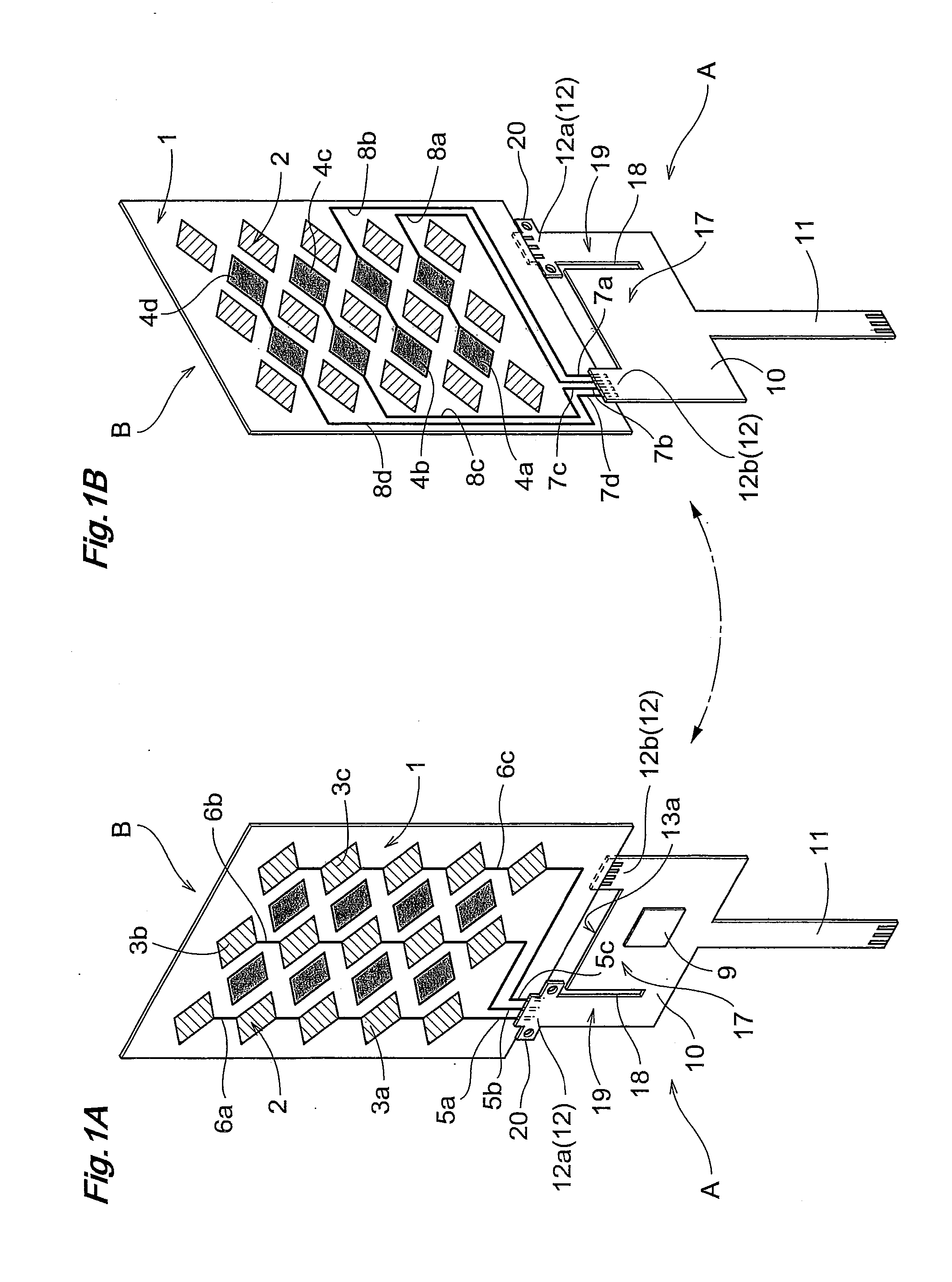
[0030]FIGS. 1A and 1B show a flexible wiring substrate A according to the present invention, and a touch panel B as an example of an electrical instrument connected to the flexible wiring substrate A. The touch panel B has a panel substrate (an example of an electrical instrument substrate) 1 formed of glass or a PET, PEN, or other polyester resin and provided with a capacitive sensor electrode 2. A touch panel B having a single panel substrate 1 is shown in the present embodiment, but a touch panel B obtained by laminating two or more panel substrates 1 may also be used.

[0031]The sensor electrode 2 is configured by arranging a plurality of x-row electrodes 3a to 3c arranged on the front surface of the panel substrate 1, and a plurality of y-row electrodes 4a to 4d arranged on the back surface of the panel substrate 1 in a mutually orthogonal matrix shape so as to be offset in a plane.

[0032]A cover panel (not shown) formed of glass, PET resin, or the like for covering each of the x-...

embodiment 2

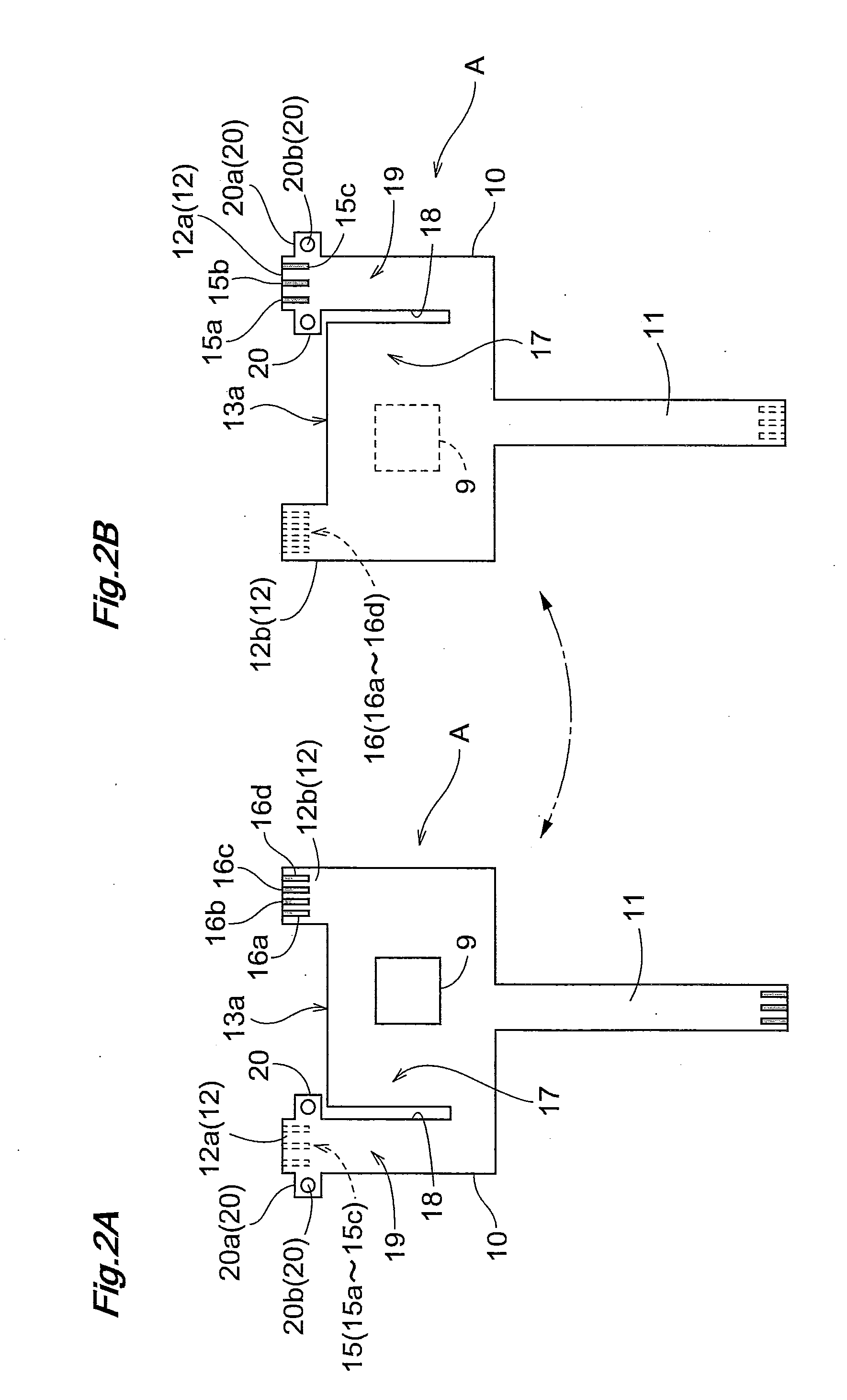
[0048]FIGS. 5A and 5B illustrate a second embodiment of the flexible wiring substrate A according to the present invention. As shown in FIG. 5A, the two protruding substrate portions 12, specifically, the first protruding substrate portion 12a and the second protruding substrate portion 12b, extend in directions opposite each other from the side edges 13a, 13b arranged opposite each other on the periphery of the rectangular wiring substrate 10.

[0049]The first protruding substrate portion 12a and the second protruding substrate portion 12b are arranged offset from each other in a direction orthogonal to the extension direction, that is, the direction along the side edges 13a, 13b; and the first protruding substrate portion 12a is extended farther than the second protruding substrate portion 12b.

[0050]The x-row wiring terminals 15 (15a to 15c) and the y-row wiring terminals 16 (16a to 16d) are arranged in parallel on the front surface of the protruding substrate portions 12 (the side...


PUM


Abstract

A plurality of protruding substrate portions (12) is extended from positions placed at an interval from each other along a peripheral edge of a wiring substrate (10). Each of the protruding substrate portions (12) is provided with wiring terminals (15), (16) electrically connected to each of a plurality of electrode terminals provided to an electrical instrument substrate. A cut-out part (18) is formed in a peripheral edge (13a) between the protruding substrate portions (12) in the wiring substrate (10).

Description

BACKGROUND OF THE INVENTION[0001]1. Field of the Invention[0002]The present invention relates to a flexible wiring substrate in which a plurality of protruding substrate portions is extended from positions placed at an interval from each other along a peripheral edge of a wiring substrate, and in which wiring terminals electrically connected to each of a plurality of electrode terminals provided to an electrical instrument substrate are provided to each of the protruding substrate portions.[0003]2. Description of the Related Art[0004]In the aforementioned flexible wiring substrate, the wiring terminals provided to each of the protruding substrate portions are electrically connected by an anisotropically conductive adhesive or other adhesive, for example, to the corresponding electrode terminals selected from among the plurality of wiring terminals provided to a touch panel substrate or other electrical instrument substrate. For example, in a conventional flexible wiring substrate su...

Claims


Application Information

Patent Timeline
IPC IPC(8): H05K1/00
CPCH05K1/028H05K1/118H05K1/147H05K1/189H05K3/361H05K2201/052H05K2203/167H05K2201/055H05K2201/09063H05K2203/0195H05K2203/1572H05K2203/166H05K2201/053
Inventor SHINODA, KOJINAKAGAWA, HIROSHI
Owner HOSIDEN CORP
Why Eureka
Try Eureka