Semiconductor Structure and Method for Making the Same

a technology of semiconductors and structures, applied in the direction of semiconductor devices, semiconductor/solid-state device details, electrical devices, etc., can solve the problems of high manufacturing cost, achieve the effects of low manufacturing cost, increase yield rate, and simplify the process

Active Publication Date: 2011-06-09
ADVANCED SEMICON ENG INC
View PDF4 Cites 103 Cited by
  • Summary
  • Abstract
  • Description
  • Claims
  • Application Information

AI Technical Summary

Benefits of technology

[0011]Therefore, in the present invention, the wafers or the chips are penetrated and electrically connected by forming only one through via, which leads to a simplified process and a low manufacturing cost. Moreover, in the present invention, the wafers and the chips are connected directly or by a bonding material, and a plurality of bumps are not needed. Therefore, the present invention avoids the disadvantage that the underfill can not completely encapsulate the bumps, and the yield rate is increased.

Problems solved by technology

For electrically connecting the chips 117, the through vias 115 are formed in each chip 117, and then the first redistribution layer (RDL) 113, the second redistribution layer (RDL) 114 and the bumps 116 are formed in each wafer 11, which leads to a high manufacturing cost.

Method used


Image

  • Semiconductor Structure and Method for Making the Same
  • Semiconductor Structure and Method for Making the Same
  • Semiconductor Structure and Method for Making the Same

Examples


first embodiment

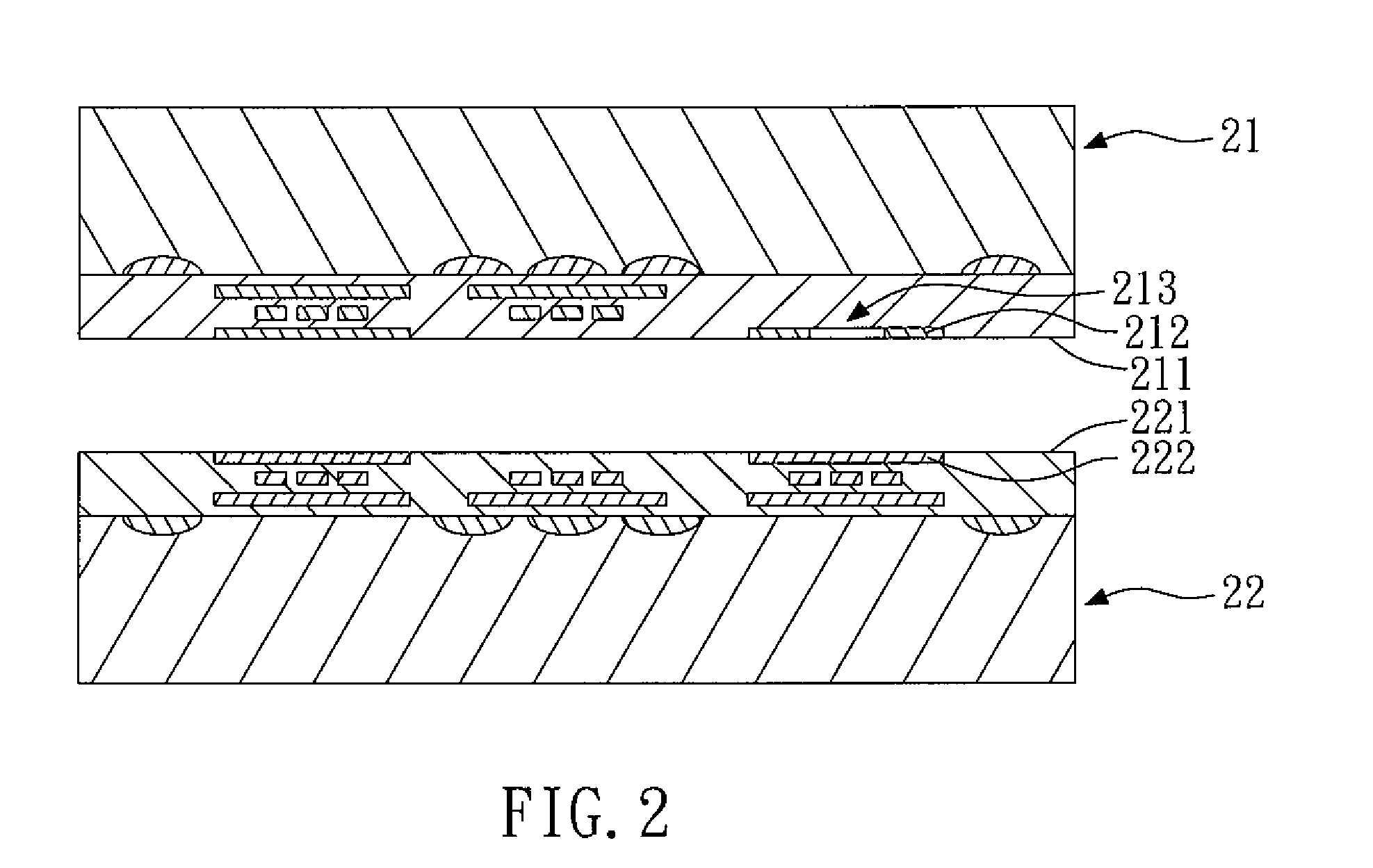
[0017]FIGS. 2 to 12 show schematic views of a method for making a semiconductor structure according to the present invention. As shown in FIG. 2, a first wafer 21 and a second wafer 22 are provided. The first wafer 21 has a first active surface 211 and at least one first conductive pad 212. The first conductive pad 212 is exposed to the first active surface 211, and has at least one through hole 213. The second wafer 22 has a second active surface 221 and at least one second conductive pad 222. The second conductive pad 222 is exposed to the second active surface 221. In this embodiment, the shape of the first conductive pad 212 and the through hole 213 thereof is circular, and the through hole 213 is disposed at the center of the first conductive pad 212, as shown in FIG. 3. However, in other embodiments, the shape of the first conductive pad 212 and the through hole 213 thereof can be square, and the through hole 213 is disposed at the center of the first conductive pad 212, as sh...

second embodiment

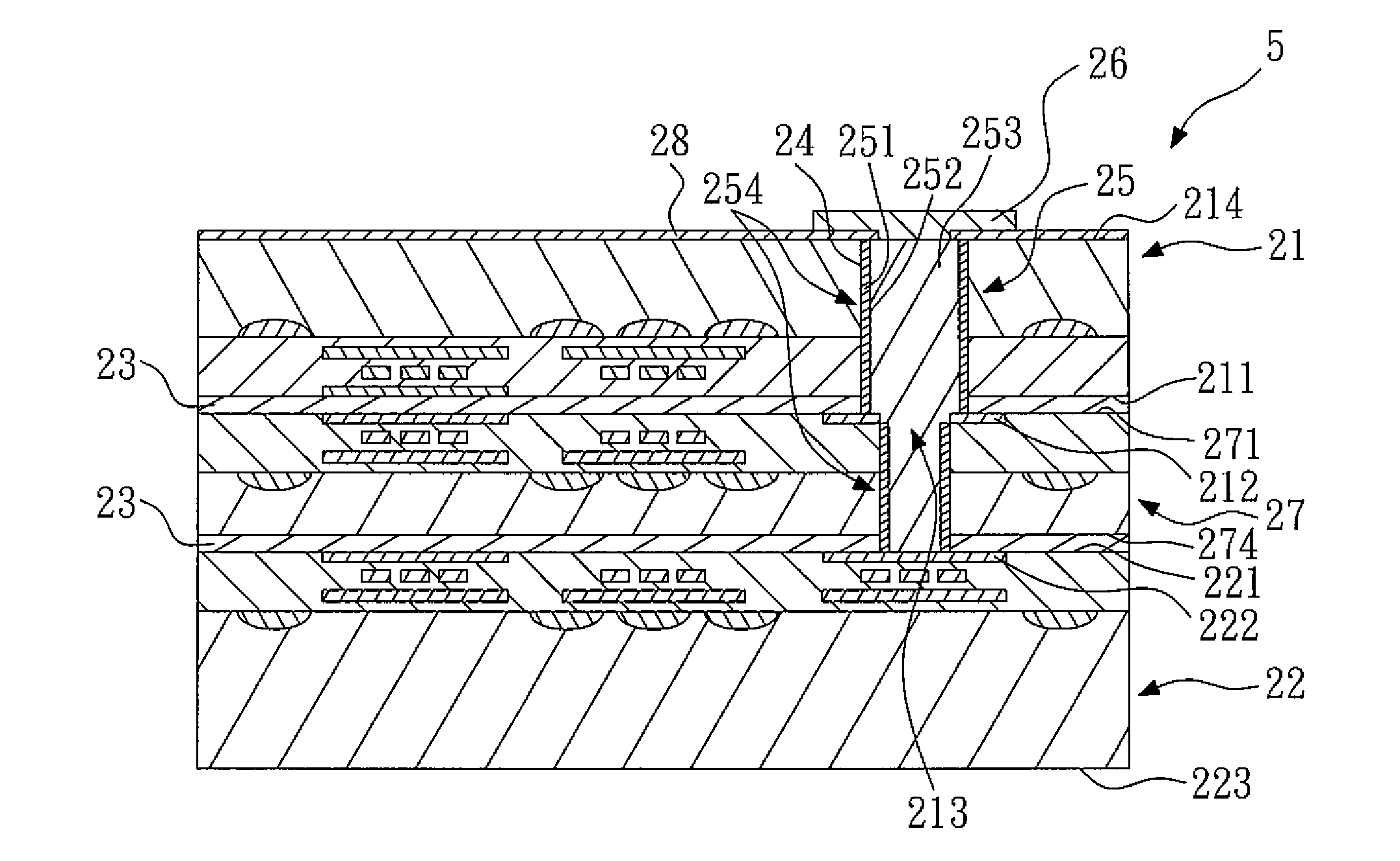
[0029]FIGS. 13 to 20 show schematic views of a method for making a semiconductor structure according to the present invention. As shown in FIG. 13, a first wafer 21, a third wafer 27, a second wafer 22 and at least one first conductive pad 212 are provided. The first wafer 21 has a first active surface 211. The third wafer 27 has a third active surface 271. The second wafer 22 has a second active surface 221 and at least one second conductive pad 222. The second conductive pad 222 is exposed to the second active surface 221. The first conductive pad 212 has at least one through hole 213, and is disposed in the first wafer 22 or the third wafer 27. In this embodiment, the first conductive pad 212 is disposed in the first wafer 22, and exposed to the first active surface 211. However, in other embodiments, as shown in FIG. 21, at least one third conductive pad 272 is further provided. The third conductive pad 272 has a through hole 273, disposed in the third wafer 27, and exposed to t...


PUM


Abstract

The present invention relates to a semiconductor structure and a method for making the same. The method includes the following steps: (a) providing a first wafer and a second wafer; (b) disposing the first wafer on the second wafer; (c) removing part of the first wafer, so as to form a groove; (d) forming a through via in the groove; and (e) forming at least one electrical connecting element on the first wafer. Therefore, the wafers are penetrated and electrically connected by forming only one conductive via, which leads to a simplified process and a low manufacturing cost.

Description

BACKGROUND OF THE INVENTION[0001]1. Field of the Invention[0002]The present invention relates to a semiconductor structure and a method for making the same, and more particularly to a semiconductor structure having a through via and a method for making the same.[0003]2. Description of the Related Art[0004]FIG. 1 shows a cross-sectional view of a conventional semiconductor structure. The conventional semiconductor structure 1 has a plurality of wafers 11 and an underfill 12. Each of the wafers 11 has a first surface 111, a second surface 112, a first redistribution layer (RDL) 113, a second redistribution layer (RDL) 114, a plurality of chips 117, a plurality of through vias 115 and a plurality of bumps 116. The first redistribution layer (RDL) 113 is disposed on the first surface 111. The second redistribution layer (RDL) 114 is disposed on the second surface 112. The chips 117 are disposed in the wafer 11, and exposed to the first surface 111 and the second surface 112. The through...

Claims


Application Information

Patent Timeline
Patent Type & Authority Applications(United States)
IPC IPC(8): H01L23/48H01L21/50
CPCH01L21/76898H01L23/481H01L25/0657H01L25/50H01L21/50H01L2225/06513H01L2225/06541H01L2924/15311H01L2224/9202H01L2224/16145H01L21/76805
Inventor WANG, MENG-JEN
Owner ADVANCED SEMICON ENG INC
Why Eureka
Try Eureka