Pixel, pixel forming method, imaging device and imaging forming method

a technology of forming method and forming method, which is applied in the direction of semiconductor/solid-state device testing/measurement, instruments, television systems, etc., can solve the problems of difficult temperature correction, inability to accurately form images of moving objects, and inability to achieve high accuracy and wide dynamic range. , the effect of high accuracy

Active Publication Date: 2011-06-09
HONDA MOTOR CO LTD
View PDF39 Cites 28 Cited by
  • Summary
  • Abstract
  • Description
  • Claims
  • Application Information

AI Technical Summary

Benefits of technology

[0017]According to the present invention, an image with a wide dynamic range can be formed by utilizing outputs caused by amounts of charge which are stored in the plurality of charge storage sections of each pixel for an object in such a way that the outputs are different. Further, in the present invention, charge is stored successively in each of the plurality of charge storage sections of each pixel for its own exposure time and the successive charging operations are repeated, and then outputs caused by amounts of charge stored in the plurality of charge storage sections are obtained. Accordingly, an image of an moving object can be formed with a high accuracy.

Problems solved by technology

However, in the method in which non-linearity of a semiconductor element is used, the non-linearity is affected by temperature and in some cases correction for temperature is not easy.
Further, in the method in which images of different periods of exposure time are combined, images picked up at different time points and therefore an image of a moving object can hardly be formed with a high accuracy.
Further, an imaging device and an image forming method by which an image of a moving object with a wide dynamic range can be formed with a high accuracy have not been developed.

Method used


Image

  • Pixel, pixel forming method, imaging device and imaging forming method
  • Pixel, pixel forming method, imaging device and imaging forming method
  • Pixel, pixel forming method, imaging device and imaging forming method

Examples


first embodiment

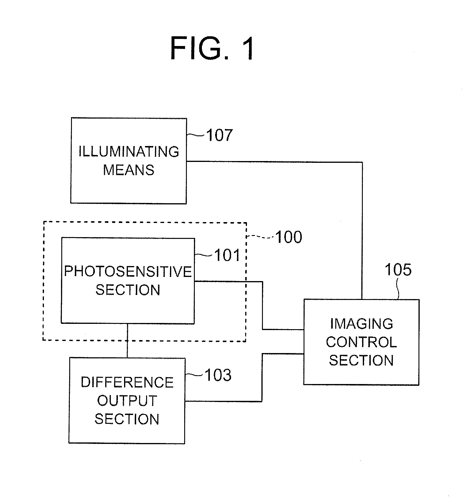
[0048]FIG. 1 shows a configuration of an imaging device according to the present invention. The imaging device includes a pixel unit 100 including a photosensitive section 101, a difference output section 103, an imaging control section 105 and illuminating means 107. The imaging control section 105 controls the photosensitive section 101 of the pixel unit 100 and the illuminating means 107 in such a way that the photosensitive section 101 of the pixel unit 100 generates a plurality of outputs under different illuminating conditions. The photosensitive section 101 of the pixel unit 100 generates a plurality of outputs under different illuminating conditions and the difference output section 103 forms an image with a wide dynamic range based on differences between the plurality of outputs. Construction and function of each component of the imaging device will be described in detail later.

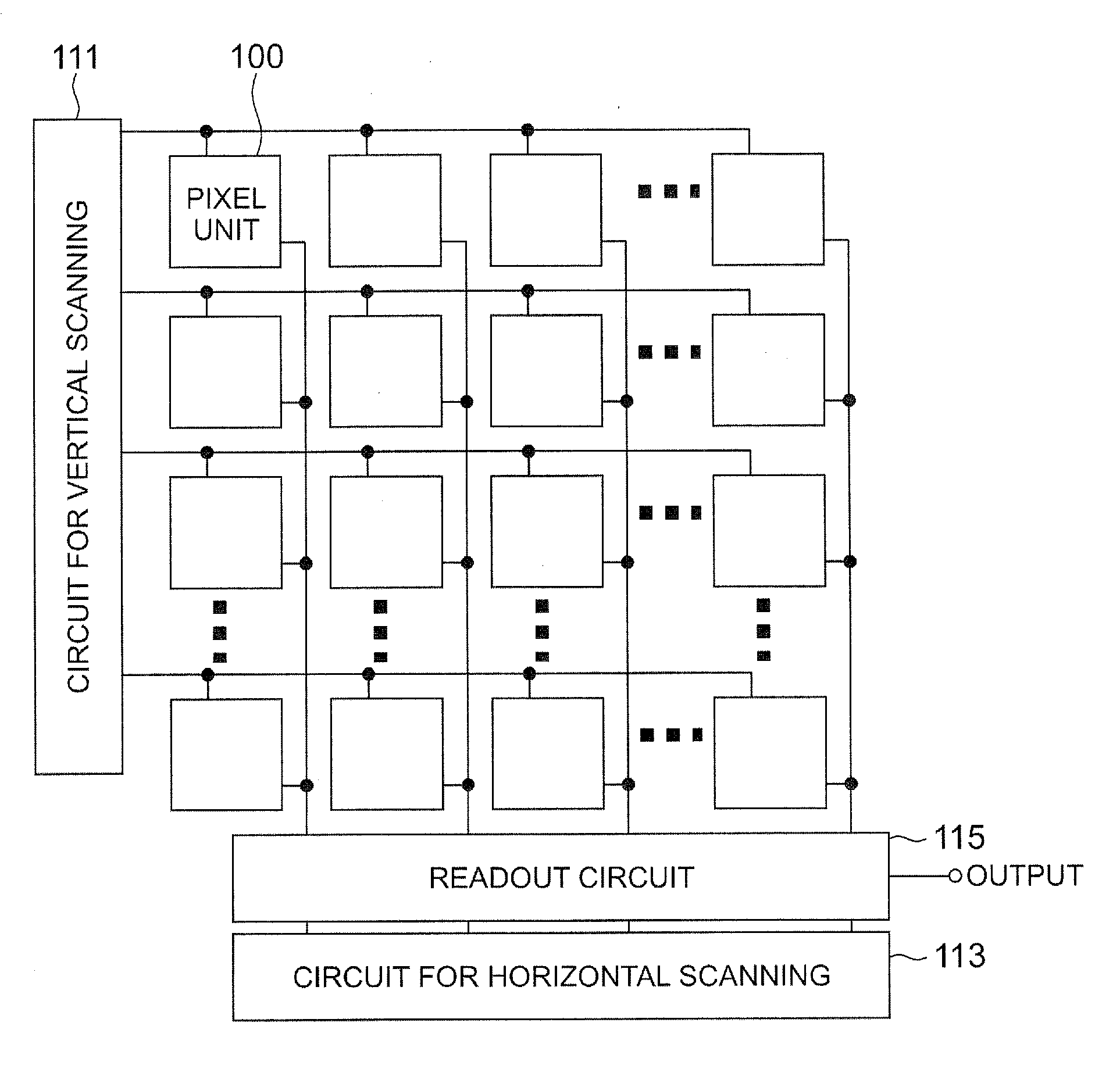
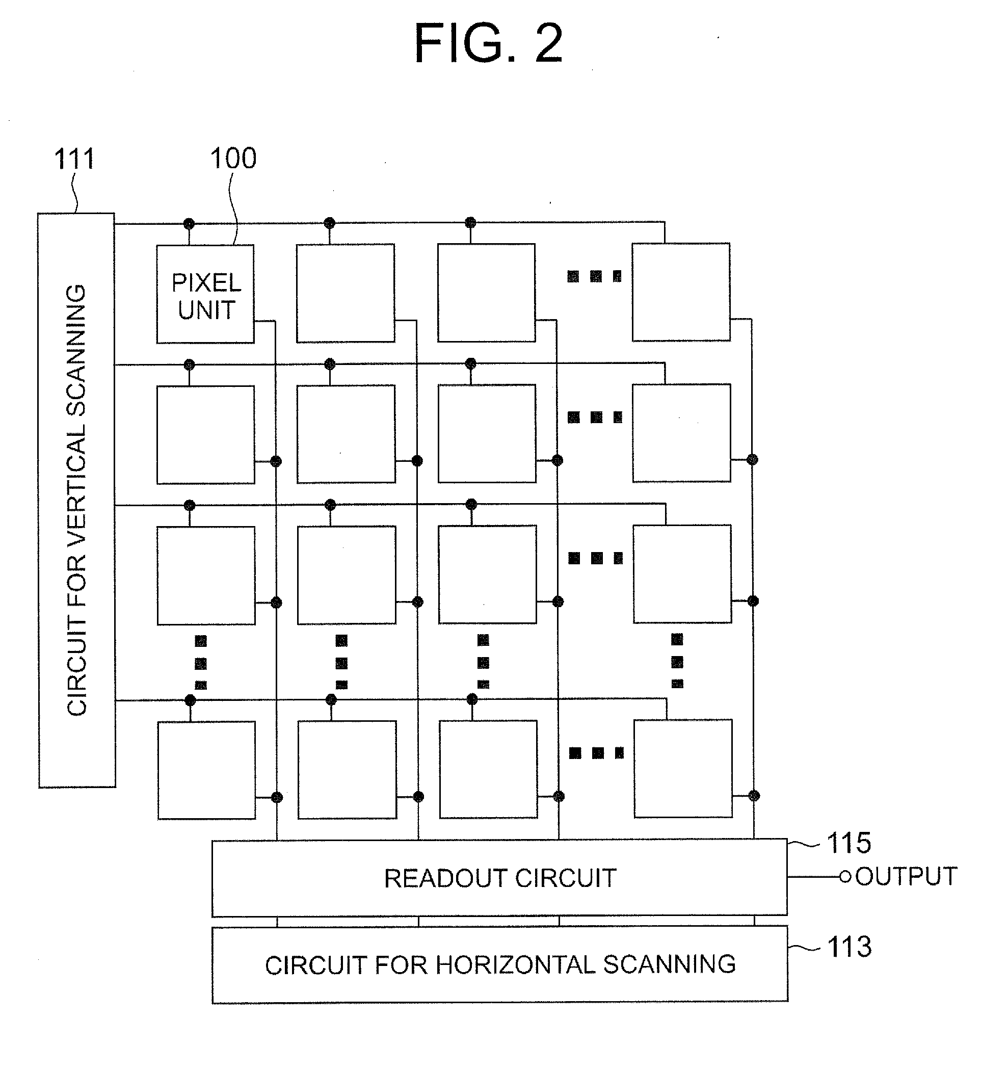
[0049]FIG. 2 shows a configuration of an array of pixel units 100 according to the present embodi...

second embodiment

[0098]FIG. 14 shows a configuration of an imaging device according to the present invention. The imaging device includes a pixel unit 200 including a photosensitive section 201, a synthesizing section 203 and an imaging control section 205. The imaging control section 205 controls the photosensitive section in such a way that the photosensitive section 201 of the pixel unit 200 forms a plurality of outputs under different conditions. The photosensitive section 201 of the pixel unit 200 forms a plurality of outputs under different conditions and the synthesizing section 203 selects appropriate outputs from the plurality of outputs to form a synthetic image. Thus, an image with a wide dynamic range is formed using outputs of the pixel unit 200. Construction and function of each component of the imaging device will be described in detail later.

[0099]FIG. 2 shows a configuration of an array of the pixel units 100. Like conventional pixel arrays, outputs of the array of the pixel units 1...


PUM


Abstract

A pixel is provided with a photodiode region which includes a photoelectric conversion portion for receiving light and generating electrons, and a charge storage portion for storing electric charge. The pixel is configured in such a manner that an electron exclusion region is provided in the photodiode region with the diameter of a circle having the maximum diameter among circles that can exist in the surface of a region through which electrons can pass in the photodiode region as the width of an electron passage region in the photodiode region, and the width of the electron passage region is smaller than when the electron exclusion region is not provided.

Description

BACKGROUND OF THE INVENTION[0001]1. Field of the Invention[0002]The present invention relates to a pixel with a short charge transfer time, a forming method thereof, an imaging device and an image forming method by which an image with a wide dynamic range can be formed.[0003]2. Background Art[0004]Conventionally, a relationship between a shape of a photodiode region of a pixel and charge transfer time has not been clear. A conventional pixel is described in Patent Document 1, for example.[0005]Methods for forming a pixel with a wide dynamic range include that in which non-linearity of a semiconductor element is used (for example, Patent Document 2) and that in which images of different periods of exposure time are combined (for example, Non-Patent Document 1). However, in the method in which non-linearity of a semiconductor element is used, the non-linearity is affected by temperature and in some cases correction for temperature is not easy. Further, in the method in which images of...

Claims


Application Information

Patent Timeline
Patent Type & Authority Applications(United States)
IPC IPC(8): H04N5/335H01L31/0352H01L31/18H04N5/355H04N5/3745
CPCH01L27/14603H01L27/14609H01L27/1461H04N5/3745H04N5/37452H04N5/3559H04N25/59H04N25/771H04N25/77
Inventor AOYAMA, CHIAKI
Owner HONDA MOTOR CO LTD
Why Eureka
Try Eureka