Method of fabricating organic light emitting diode display device

Active Publication Date: 2011-06-09
SAMSUNG DISPLAY CO LTD
View PDF5 Cites 0 Cited by
  • Summary
  • Abstract
  • Description
  • Claims
  • Application Information

AI Technical Summary

Benefits of technology

[0008]Aspects of the present invention provide a method of fabricating an OLED display

Problems solved by technology

If the separation of the donor film from the acceptor substrate is not carried out smoothly, lifting of the transferred transfer layer from the acceptor substrate may occur due to adhesion between the transfer layer and the donor film and due to the tensile force applied to the donor film.

Method used


Image

  • Method of fabricating organic light emitting diode display device
  • Method of fabricating organic light emitting diode display device
  • Method of fabricating organic light emitting diode display device

Examples


Embodiment Construction

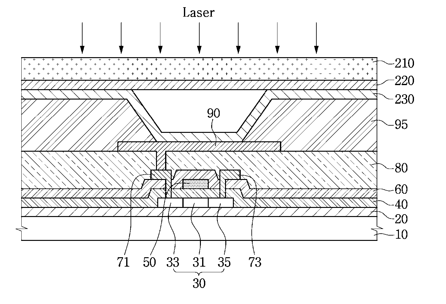
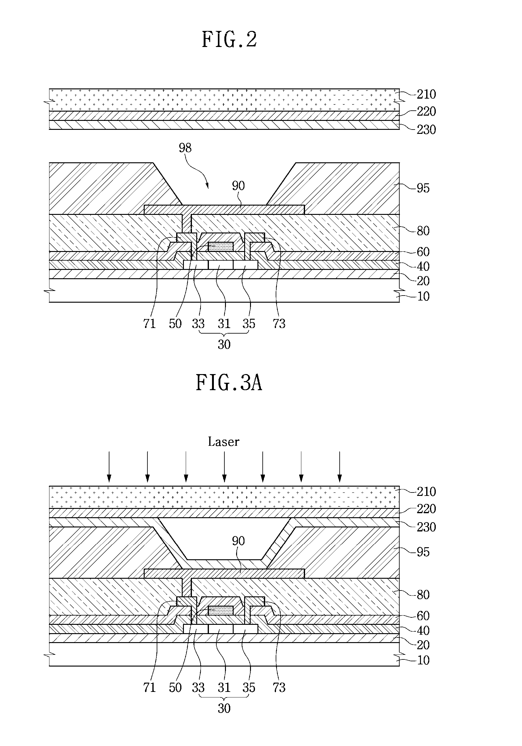
[0016]Reference will now be made in detail to the present embodiments of the present invention, examples of which are illustrated in the accompanying drawings, wherein like reference numerals refer to the like elements throughout. The embodiments are described below in order to explain the present invention by referring to the figures Moreover, it is to be understood that where is stated herein that one layer is “formed on” or “disposed on” a second layer, the first layer may be formed or disposed directly on the second layer or there may be intervening layers between the first layer and the second layer. Further, as used herein, the term “formed on” is used with the same meaning as “located on” or “disposed on” and is not meant to be limiting regarding any particular fabrication process.

[0017]Hereinafter, a method of fabricating an OLED display device according to an exemplary embodiment of the present invention will be described with reference to the accompanying drawings. Accordi...


PUM


Abstract

An organic layer of an organic light emitting diode (OLED) display device is formed by transferring a transfer layer of a donor film to aligned pixel openings in a pixel defining region of the OLED display device such that the organic layer is formed in the pixel openings. Each aligned pixel opening has a pair of long sides and a pair of short sides, and the transferring of the transfer layer is performed by applying tensile force to the donor film in a direction perpendicular to the short sides of the pixel openings.

Description

CROSS-REFERENCE TO RELATED APPLICATIONS[0001]This application claims the benefit of Korean Patent Application No. 10-2009-0120649, filed Dec. 7, 2009, in the Korean Intellectual Property Office, the disclosure of which is hereby incorporated herein by reference in its entirety.BACKGROUND OF THE INVENTION[0002]1. Field of the Invention[0003]Aspects of the present invention relate to a method of fabricating an organic light emitting diode (OLED) display device, and more particularly, to a method of fabricating an OLED display device in which an organic layer is formed by transferring a transfer layer.[0004]2. Description of the Related Art[0005]Generally, an OLED display device is fabricated by forming an anode on an insulating substrate, forming an organic layer on the anode, and forming a cathode on the organic layer. The organic layer includes an emitting layer, and may further include at least one of a hole transport layer, a hole injection layer, an electron transport layer, a ho...

Claims


Application Information

Patent Timeline
IPC IPC(8): H01L51/40
CPCH01L51/56H01L51/0013H10K71/18H10K71/00H10K71/60H05B33/10
Inventor SUN, JIN-WONKANG, TAE-MINLEE, SANG-BONG
Owner SAMSUNG DISPLAY CO LTD
Why Eureka
Try Eureka