Light emitting device

a technology of light-emitting devices and light-emitting tubes, which is applied in the direction of semiconductor devices, electrical equipment, basic electric elements, etc., can solve the problems of non-uniform emission intensity distribution of such devices, and achieve the effects of suppressing color unevenness, reducing emission intensity distribution differences, and easy control

Active Publication Date: 2011-06-23
NICHIA CORP
View PDF5 Cites 90 Cited by
  • Summary
  • Abstract
  • Description
  • Claims
  • Application Information

AI Technical Summary

Benefits of technology

[0008]Accordingly, an object of the present invention is to provide a novel light emitting device that can improve both the color unevenness and light extracting efficiency of the light emitting device at the same time.
[0010]First, the difference in emission intensity distribution between semiconductor light emitting element and fluorescent material layer will be described. The emission intensity distribution involves a distribution caused by the position within the light emitting surface (hereafter referred to as in-surface distribution) and a distribution caused by the direction of viewing the light emitting surface (hereafter referred to as light distribution characteristic). The primary light emitted from the semiconductor light emitting element such as light emitting diode is surface emission from the semiconductor layer, which is subjected to the influence of light blocking by an electrode, so that the in-surface distribution tends to be generated depending on the die shape and the electrode shape, while the light distribution characteristic tends to be non-uniform. Also because the primary light of the semiconductor light emitting element emits after passing through the fluorescent material layer, the in-surface distribution and the light distribution characteristic of light emission of the semiconductor light emitting element are affected also by means of the arrangement, thickness, shape or the like of the fluorescent material layer. On the other hand, the fluorescent material layer emits the secondary light of a longer wavelength by absorbing a part of the primary light of the light emitting diode, and therefore there is no need for complicated structure of electrode or the like, thus providing a high degree of freedom in the design of arrangement, thickness and shape. As a result, the in-surface distribution of the fluorescent material layer can be relatively freely controlled and the light distribution characteristic of the fluorescent material layer can be easily made uniform by adjusting the arrangement, thickness and shape or the like of the fluorescent material layer.
[0016]The present invention is based on the notice of the fact that emission intensity distribution of the fluorescent material layer can easily be controlled by means of the arrangement, thickness and shape or the like of the fluorescent material layer, while emission intensity distribution of the semiconductor light emitting element tends to be non-uniform fundamentally and is affected also as the light passes through fluorescent material layer. Accordingly the present invention is characterized by the capability to selectively scatter the primary light of the semiconductor light emitting element by controlling the mean particle size D of the particles, dispersed in the transparent medium, within a predetermined range. To selectively scatter the primary light of the semiconductor light emitting element means scattering the primary light of the semiconductor light emitting element significantly more strongly than the secondary light of longer wavelength of the fluorescent material layer. It is preferable that the primary light is scattered twice more strongly than the secondary light.
[0017]Selectively scattering the primary light of the semiconductor light emitting element makes it possible to selectively control the emission intensity distribution of the semiconductor light emitting element. Therefore, since the present invention enables it to appropriately control the emission intensity distribution of the fluorescent material layer by means of the arrangement, thickness and shape thereof, and control the emission intensity distribution of the semiconductor light emitting element by means of the scattering layer independently of the emission intensity distribution of the fluorescent material layer, it is made possible to suppress the color unevenness by reducing the difference in emission intensity distribution between the semiconductor light emitting element and the fluorescent material layer. Also according to the present invention, since light of the fluorescent material layer is not scattered strongly by the scattering layer, it is made possible to reduce the light that returns to the semiconductor light emitting element and the fluorescent material layer due to excessive scattering, and suppress the light extracting efficiency from decreasing. As a result, the present invention makes it possible to suppress light extracting efficiency of the light emitting device from decreasing, thereby to improve the color unevenness and provide the light emitting device that is bright and has less color unevenness.
[0018]The particles used in the present invention also have an effect of increasing the refractive index and the heat conductivity of the material in which the particles are dispersed, while suppressing excessive scattering of visible light therein. Accordingly, reflection loss may also be reduced by dispersing the particles in various materials other than the scattering layer. For example, the particles may be dispersed in the fluorescent material layer per se, an adhesive that fastens the fluorescent material layer onto the semiconductor light emitting element and the die-bonding material that fastens the semiconductor light emitting element. The particles dispersed in these materials may have the same as or different from that of the particles dispersed in the scattering layer, as long as the mean particle size satisfies Inequality 1.
[0019]As described above, according to the present invention, in the light emitting device including the semiconductor light emitting element and the fluorescent material layer, since the scattering layer that scatters the primary light of the semiconductor light emitting element more strongly than the secondary light of the fluorescent material layer is provided, it is made possible to reduce the return light caused by excessive scattering of the secondary light of the fluorescent material layer, and suppress the light extracting efficiency from decreasing, while suppressing the color unevenness caused by the difference in emission intensity distribution between the semiconductor light emitting element and the fluorescent material layer. As a result, the light emitting device that emits bright light with less color unevenness can be achieved.

Problems solved by technology

Light emission distribution exhibited by the semiconductor light emitting element is surface emission from the semiconductor layer, and therefore the emission intensity distribution thereof tends to be non-uniform, and changes significantly with the quantity of fluorescent material disposed around the semiconductor light emitting element.

Method used


Image

  • Light emitting device
  • Light emitting device
  • Light emitting device

Examples


first embodiment

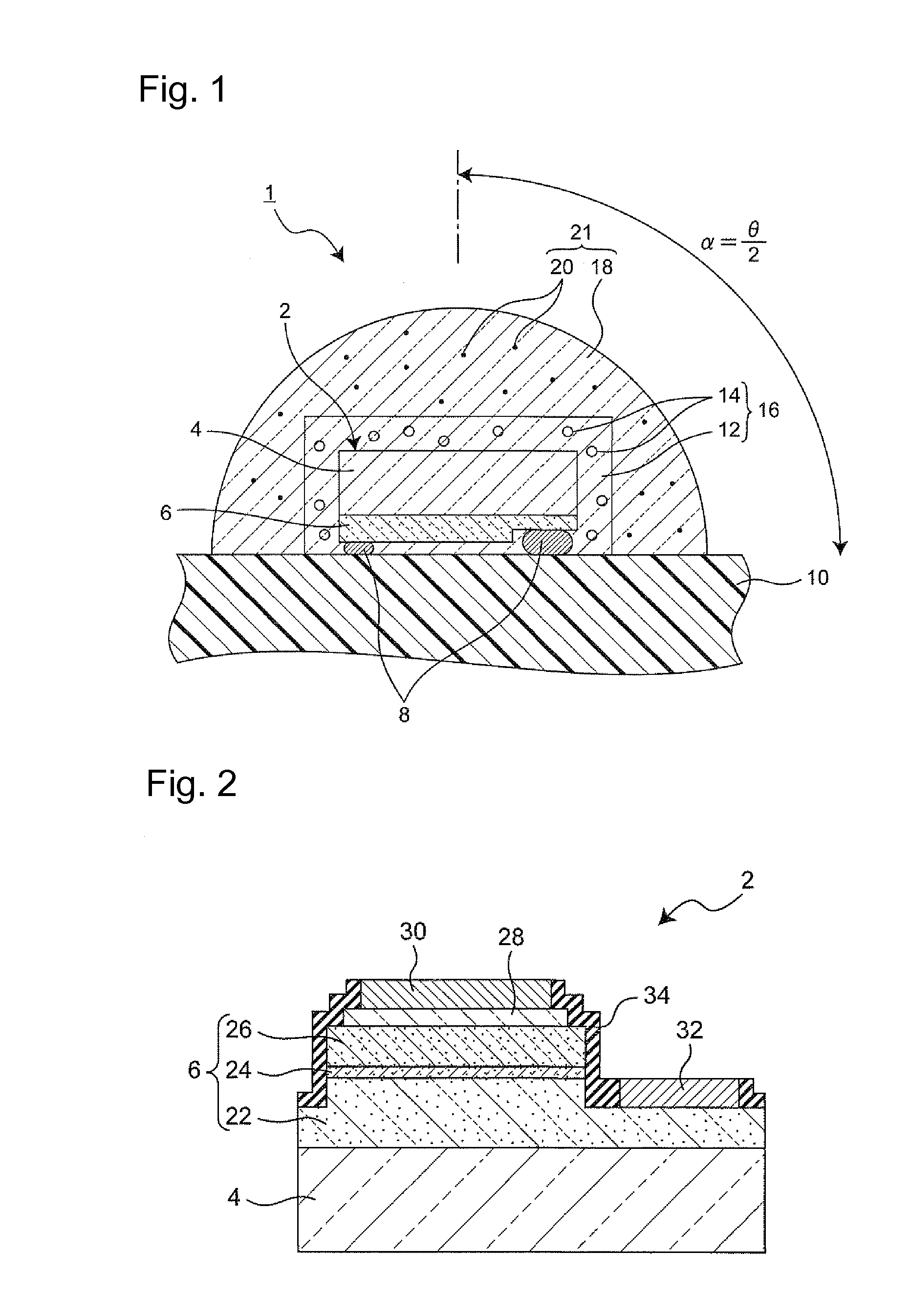
[0033]FIG. 1 is a schematic sectional view showing a light emitting device 1 according to the first embodiment of the present invention. A semiconductor light emitting element 2 is fastened via a solder bump 8 on a mounting substrate 10, and the periphery is coated by a fluorescent material layer 16 having substantially uniform thickness. The semiconductor light emitting element 2 is constituted by forming a semiconductor layer 6, that has a light emitting layer capable of emitting blue light, on a substrate 4 of square shape in plan view, and is flip-chip mounted with the semiconductor layer 6 facing down and the substrate 4 facing up. The fluorescent material layer 16 is formed by dispersing fluorescent material particles 14 in a transparent fluorescent material holding member 12, so that the fluorescent material particles 14 absorb a part of blue light (primary light) emitted by the semiconductor light emitting element 2 and emit light of longer wavelength such as yellow light (s...

second embodiment

[0068]FIG. 4 is a sectional view showing a light emitting device according to the second embodiment of the present invention. The light emitting device 1 shown in FIG. 4 comprises two layers; a first fluorescent material layer 16a that emits red light and a second fluorescent material layer 16b that emits yellow light, disposed in this order from the inside. This constitution enables it to make the light emitting device that emits light with higher red component and higher mean color rendering index Ra than in the case of forming only the fluorescent material layer 16 that emits yellow light. The light emitting device having higher mean color rendering index Ra is suited for illumination applications. Increasing the red component also enables it to make the light emitting device that emits light of warm white. This embodiment is similar to the first embodiment in other respects.

[0069]The first fluorescent material layer 16a preferably contains fluorescent material particles 14a that...

third embodiment

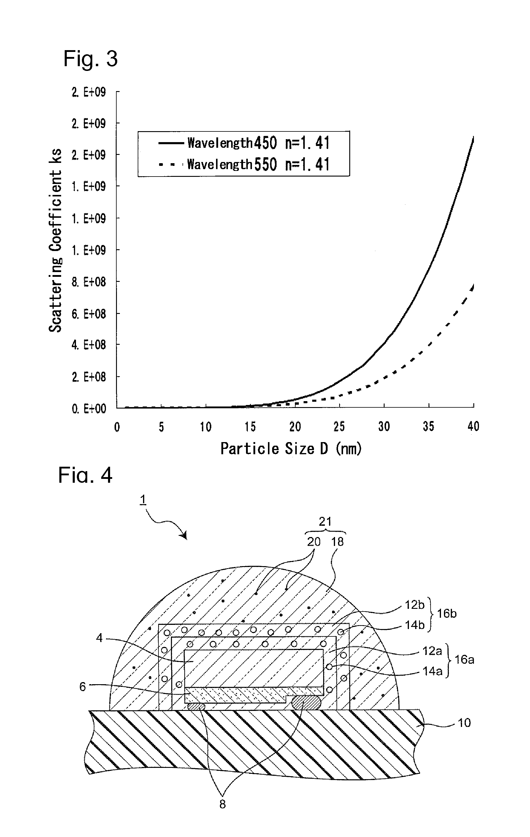
[0074]FIG. 5 is a sectional view showing a light emitting device according to the third embodiment of the present invention. The light emitting device 1 shown in FIG. 5 has particles 20 formed from an inorganic material having high refractive index dispersed also in the fluorescent material layer 16. This embodiment is similar to the first embodiment except for this respect.

[0075]Refractive index of the fluorescent material layer 16 can be increased by dispersing the particles 20 having a higher refractive index than that of the fluorescent material holding member 12. This increases the critical angle at which total reflection occurs in the interface between the substrate 4 and the fluorescent material layer 16 and the interface between the fluorescent material layer 16 and the scattering layer 21, thereby decreasing the reflection loss at the interfaces. When the particles 20 formed from an inorganic material are dispersed also in the fluorescent material layer 16, the heat conduct...


PUM


Abstract

To provide a light emitting device capable of improving both color unevenness and an emission output power.The light emitting device includes a semiconductor light emitting element including a semiconductor layer that emits primary light; and a fluorescent material layer disposed on the light emitting side of the semiconductor light emitting element, that absorbs a part of the primary light and emits secondary light having a wavelength longer than that of the primary light; and emits light of blended color of the primary light and the secondary light of the light emitting element, and further includes a scattering layer in which particles having a mean particle size D that satisfies the inequality: 20 nm<D≦0.4×λ / π are dispersed in a transparent medium.

Description

BACKGROUND OF THE INVENTION[0001]1. Field of the Invention[0002]The present invention relates to a light emitting device capable of color-mixing light emitted by a light emitting element and light obtained through wavelength conversion of a part of the original light, thereby emitting light of a different color.[0003]2. Description of the Related Art[0004]A semiconductor light emitting element such as light emitting diode is small in size, has high power efficiency and emits light with clear color. The semiconductor light emitting element also has such advantages as excellent startup performance and high durability to vibration and repetitive operations of turning on and off. Light emitting devices have been developed that are capable of emitting light of various colors by combining the primary light of the semiconductor light emitting element and a fluorescent material capable of emitting secondary light of a different wavelength through excitation by the primary light, based on th...

Claims


Application Information

Patent Timeline
Patent Type & Authority Applications(United States)
IPC IPC(8): H01L33/50
CPCH01L33/50H01L33/505H01L33/54H01L2933/0091H01L33/502H01L33/644H01L2224/8592H01L2224/13H01L2224/48091H01L2224/48247H01L2924/00014H01L2924/181H01L2224/48257H01L2924/00012
Inventor ICHIKAWA, MASATSUGU
Owner NICHIA CORP
Why Eureka
Try Eureka