
Photon imaging system for detecting defects in photovoltaic devices, and method thereof

a photovoltaic device and imaging system technology, applied in the field of photovoltaic devices, can solve the problems of substantial power consumption for the operation of light sources, and the inability to provide any information about the reliability of solar modules

Inactive Publication Date: 2011-06-23
FIRST SOLAR INC (US)
View PDF7 Cites 21 Cited by
  • Summary
  • Abstract
  • Description
  • Claims
  • Application Information

AI Technical Summary

Benefits of technology

[0007]In accordance with another exemplary embodiment of the present invention, a computer readable media to enable a processor device to determine at least one defect in the at least one photovoltaic device is disclosed.

Problems solved by technology

This conventional technique provides information related to the power conversion efficiency of the solar modules but does not provide any information about the reliability of the solar module.
Moreover, substantial power is consumed for the operation of the light source.

Method used


Image

  • Photon imaging system for detecting defects in photovoltaic devices, and method thereof
  • Photon imaging system for detecting defects in photovoltaic devices, and method thereof
  • Photon imaging system for detecting defects in photovoltaic devices, and method thereof

Examples


Embodiment Construction

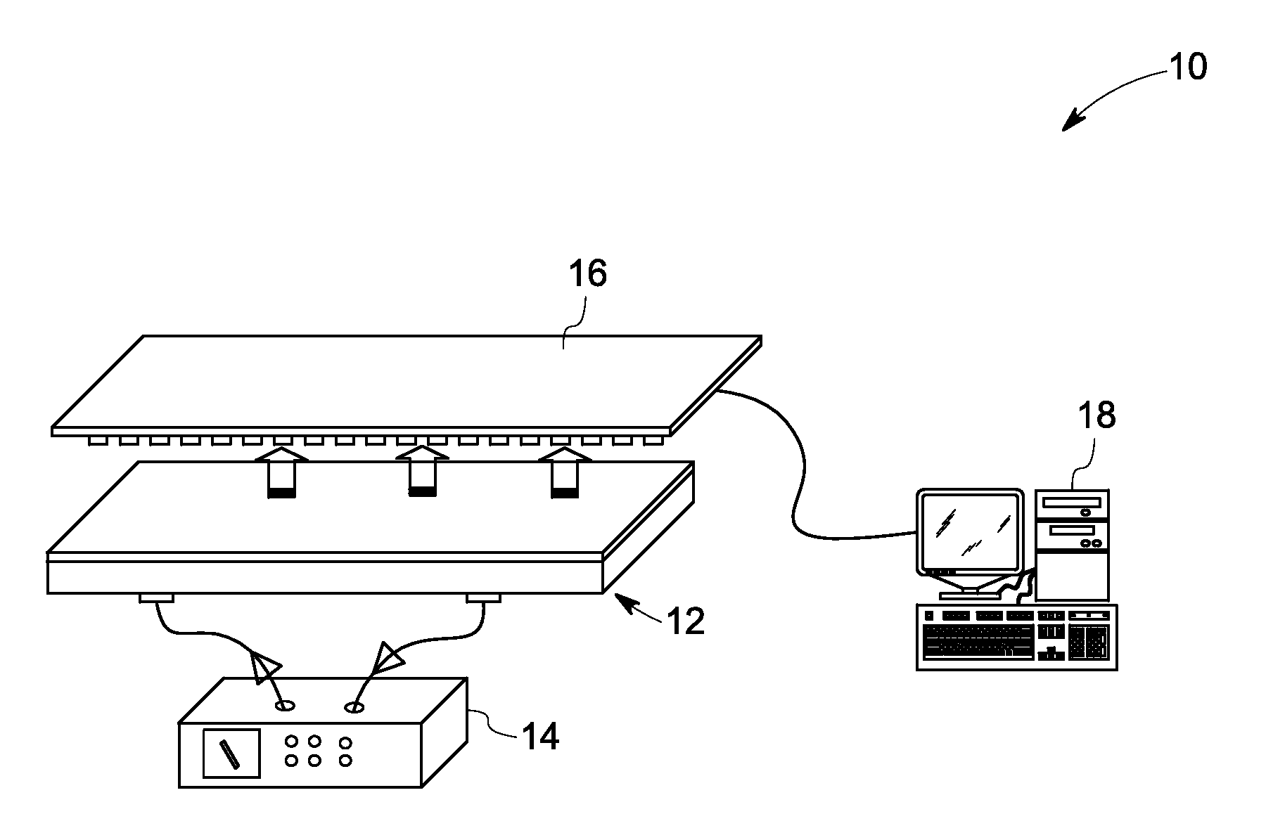
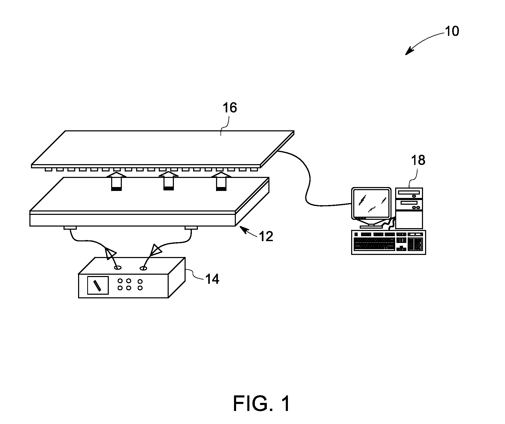
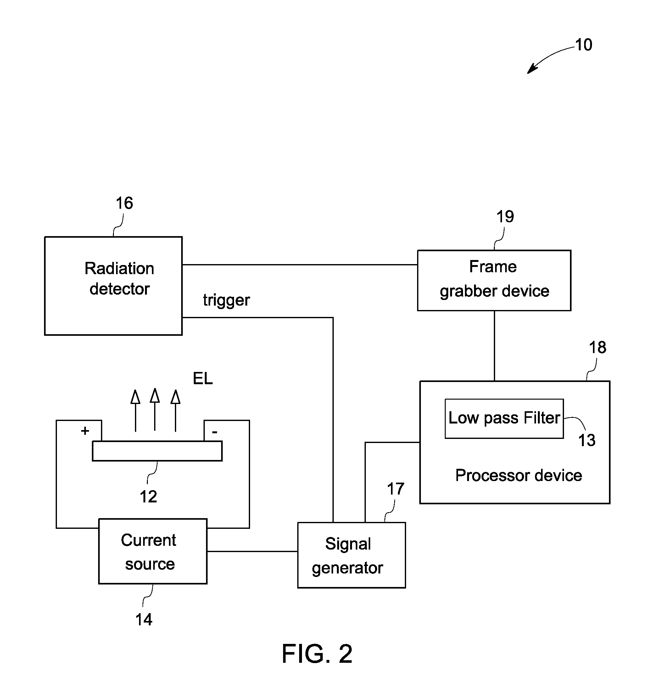
[0018]As discussed in detail below, embodiments of the present technique provide a diagnostic method for determining at least one defect in one or more photovoltaic device, for example a thin-film photovoltaic module. The method includes supplying current to at least one photovoltaic device via a current source and detecting emitted photon radiations from the at least one photovoltaic device via a radiation detector. The method also includes outputting a signal corresponding to the detected emitted photon radiations from the radiation detector to a processor device, and processing the signal corresponding to the detected emitted photon radiations via the processor device to generate one or more two-dimensional photon images. The method further includes analyzing the one or more two-dimensional photon images to determine at least one defect in the at least one photovoltaic device. In accordance with a specific embodiment, a diagnostic system for determining at least one defect in one...


PUM

PropertyMeasurementUnit
Electrical resistanceaaaaaaaaaa
Band gapaaaaaaaaaa
Currentaaaaaaaaaa

Abstract

A method includes supplying current to at least one photovoltaic device via a current source and detecting emitted photon radiations from the at least one photovoltaic device via a radiation detector. The method also includes outputting a signal corresponding to the detected emitted photon radiations from the radiation detector to a processor device, and processing the signal corresponding to the detected emitted photon radiations via the processor device to generate one or more two-dimensional photon images. The method further includes analyzing the one or more two-dimensional photon images to determine at least one defect in the at least one photovoltaic device.

Description

BACKGROUND[0001]The invention relates generally to photovoltaic devices, and more particularly, to an imaging system for detecting defects in photovoltaic cells, modules, and method thereof.[0002]Solar energy is considered as an alternate source of energy relative to other forms of energy. Solar energy conversion systems are used to convert solar energy into electrical energy. The solar energy conversion system typically includes photovoltaic modules, photoelectric cells, or solar cells that convert solar energy into electrical energy for immediate use or for storage and subsequent use. Conversion of solar energy into electrical energy includes reception of light, such as sunlight, at a solar cell, absorption of sunlight into the solar cell, generation and separation of positive and negative charges creating a voltage in the solar cell, and collection and transfer of electrical charges through a terminal coupled to the solar cell.[0003]In solar module manufacturing line, it is helpf...

Claims


Application Information

Patent Timeline
IPC IPC(8): G01N21/88
CPCG01N21/66H02S50/10G01R31/308G01N21/9505Y02E10/50
Inventor AHMAD, FAISAL RAZISULIMA, OLEGNAGARKAR, KAUSTUBH RAVINDRAZHAO, RI-ANBRAY, JAMES WILLIAM
Owner FIRST SOLAR INC (US)
Learn More