Stack package

a technology of stack and package, applied in the field of stack package, can solve the problems of high integration of memory chips that requires both high precision techniques, and the stack itself may be impossible, so as to achieve the effect of ensuring structural stability

Active Publication Date: 2011-06-30
SK HYNIX INC
View PDF31 Cites 32 Cited by
  • Summary
  • Abstract
  • Description
  • Claims
  • Application Information

AI Technical Summary

Benefits of technology

[0008]Embodiments of the present invention include a stack package which can secure structural stability even when an upwardly stacked chip has a size greater than a downwardly disposed chip.

Problems solved by technology

However, high integration of a memory chip requires both high precision techniques, such as a technique for attaining a fine line width, and a lengthy development period.
When manufacturing a stack package such that electrical connections between upper and lower semiconductor chips are formed through through-electrodes, if the size of a downwardly positioned chip (hereinafter referred to as a “lower chip”) and an upwardly positioned chip (hereinafter referred to as an “upper chip”) are different, defects are likely to occur.
For example, in the event that the lower chip has a size smaller than the upper chip, the stack may be implemented while the upper chip is in a structurally unstable state, and the stack itself may be impossible.

Method used


Image

  • Stack package
  • Stack package
  • Stack package

Examples


Embodiment Construction

[0038]Hereafter, specific embodiments of the present invention will be described in detail with reference to the accompanying drawings.

[0039]It is to be understood herein that the drawings are not necessarily to scale and in some instances proportions may have been exaggerated in order to more clearly depict certain features of the invention.

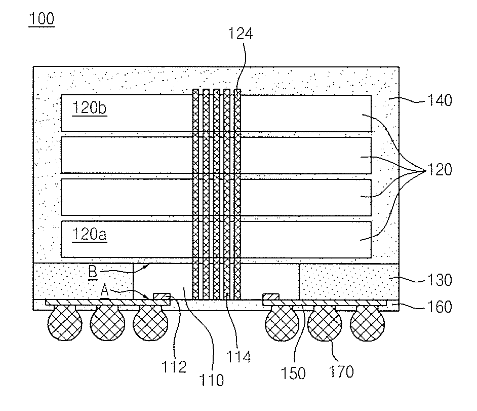
[0040]FIG. 1 is a cross-sectional view showing a stack package in accordance with a first embodiment of the present invention.

[0041]Referring to FIG. 1, a stack package 100 in accordance with an embodiment of the present invention includes a first semiconductor chip 110, a molding part 130 which surrounds the side surfaces of the first semiconductor chip 110, and one or more second semiconductor chips 120 which are stacked on the first semiconductor chip 110 and the molding part 120.

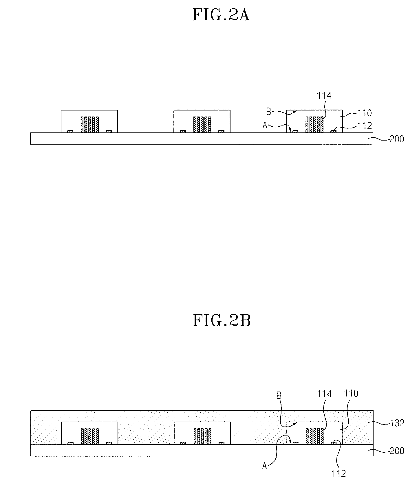
[0042]In the embodiment, the first semiconductor chip 110 has a first surface A on which bonding pads 112 are disposed, and a second surface B which faces away from ...


PUM


Abstract

A stack package includes a first semiconductor chip possessing a first size and one or more second semiconductor chips possessing a second size greater than the first size. The first semiconductor chip has a first surface on which bonding pads are disposed, a second surface which faces away from the first surface, and first through-electrodes which pass through the first surface and the second surface. The one or more second semiconductor chips are stacked on the second surface of the first semiconductor chip and have second through-electrodes which are electrically connected to the first through-electrodes. A molding part abuts one or more side surfaces of the first semiconductor chip such that a total size including the first size and a size of the molding part is equal to or greater than the second size.

Description

CROSS-REFERENCE TO RELATED APPLICATIONS[0001]The present application claims priority to Korean patent application number 10-2009-0135201 filed on Dec. 31, 2009, which is incorporated herein by reference in its entirety.BACKGROUND OF THE INVENTION[0002]The present invention relates generally to semiconductor technology, and more particularly, to a stack package.[0003]In order to accommodate the demands for miniaturization and high performance, new techniques for providing a semiconductor module of high capacity are required. One method for providing a semiconductor module of high capacity is to manufacture a highly integrated memory chip. High integration of a memory chip is accomplished by integrating an increased number of cells in the already limited space of the semiconductor chip.[0004]However, high integration of a memory chip requires both high precision techniques, such as a technique for attaining a fine line width, and a lengthy development period. With these limitations in...

Claims


Application Information

Patent Timeline
Patent Type & Authority Applications(United States)
IPC IPC(8): H01L25/065H01L23/36H01L23/52
CPCH01L21/561H01L21/568H01L2924/0002H01L24/96H01L2224/0401H01L2224/73204H01L2224/32225H01L2224/16225H01L24/19H01L2924/014H01L2924/01074H01L2924/01006H01L2924/01005H01L2924/15311H01L2924/01078H01L2924/01047H01L2924/01033H01L21/6835H01L21/76898H01L23/3128H01L23/3135H01L24/11H01L24/13H01L24/16H01L24/24H01L24/48H01L24/73H01L24/81H01L24/94H01L25/0657H01L2224/0557H01L2224/13009H01L2224/16145H01L2224/32188H01L2224/4824H01L2224/83102H01L2224/92125H01L2225/06541H01L2924/01029H01L2924/00H01L2224/05552H01L2224/12105H01L2224/73259H01L2224/451H01L2924/181H01L2924/00014H01L24/45H01L2224/1134H01L24/97H01L2224/04105H01L2224/1703H01L2224/17181H01L2224/73257H01L2224/81005H01L2224/05599H01L23/12
Inventor KIM, JONG HOON
Owner SK HYNIX INC
Why Eureka
Try Eureka