Method for driving liquid crystal display device

a liquid crystal display and display device technology, applied in the direction of electric digital data processing, instruments, computing, etc., can solve the problems of display image deterioration, inability to keep the voltage constant between the pixel electrode and the common electrode in some cases, etc., and achieve the effect of suppressing the deterioration of the displayed imag

Inactive Publication Date: 2011-06-30
SEMICON ENERGY LAB CO LTD
View PDF17 Cites 39 Cited by
  • Summary
  • Abstract
  • Description
  • Claims
  • Application Information

AI Technical Summary

Benefits of technology

[0019]According to one embodiment of the present invention, deterioration of a displayed image can be suppressed even when the refresh rate is reduced in displaying a still image.

Problems solved by technology

However, a voltage between a pixel electrode and a common electrode cannot be kept constant in some cases because the potential of the pixel electrode is changed by the off-state current of a pixel transistor and / or leakage current from liquid crystals.
Therefore, a displayed image deteriorates because a voltage applied to the liquid crystals is changed.

Method used


Image

  • Method for driving liquid crystal display device
  • Method for driving liquid crystal display device
  • Method for driving liquid crystal display device

Examples


embodiment 1

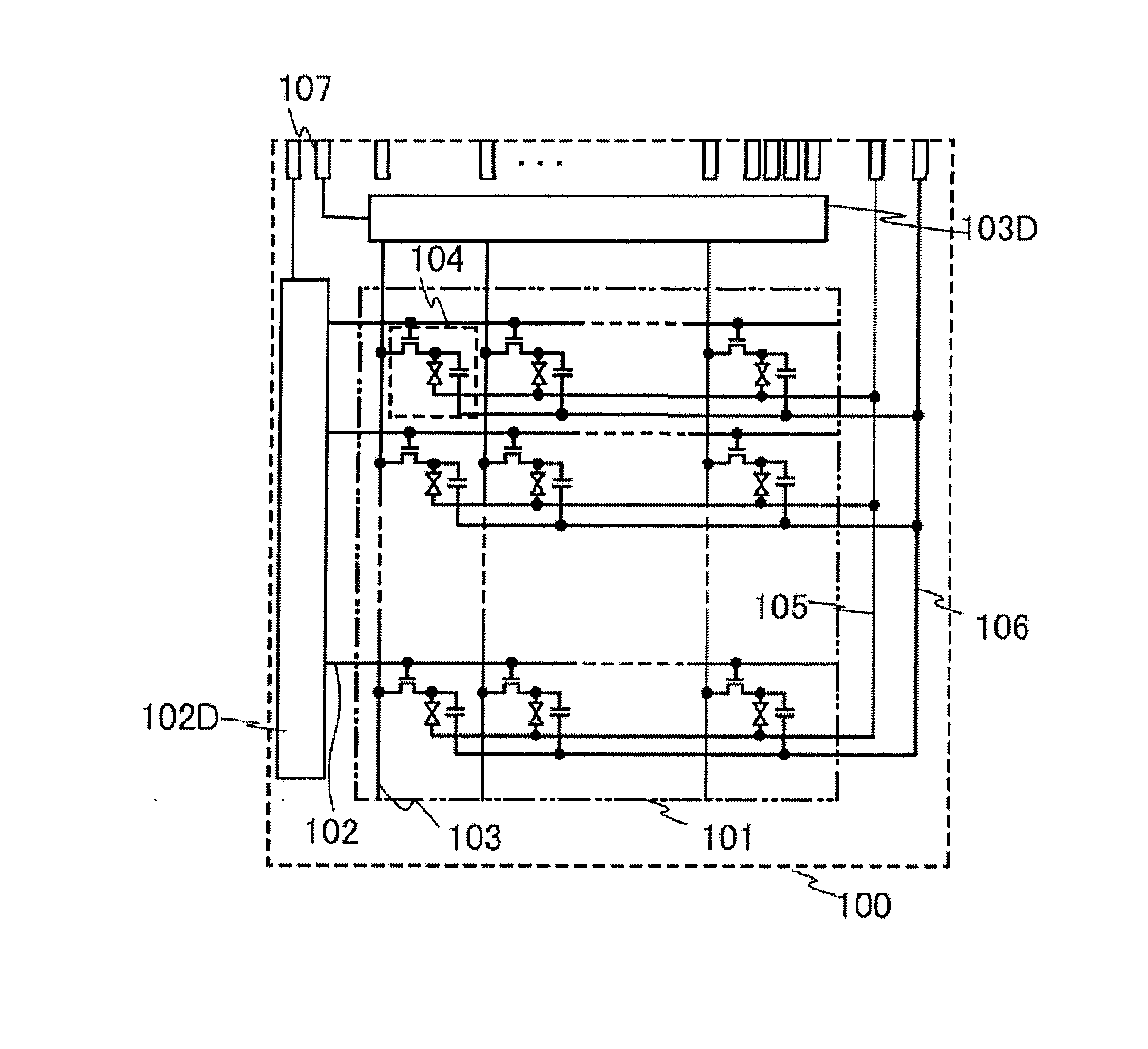
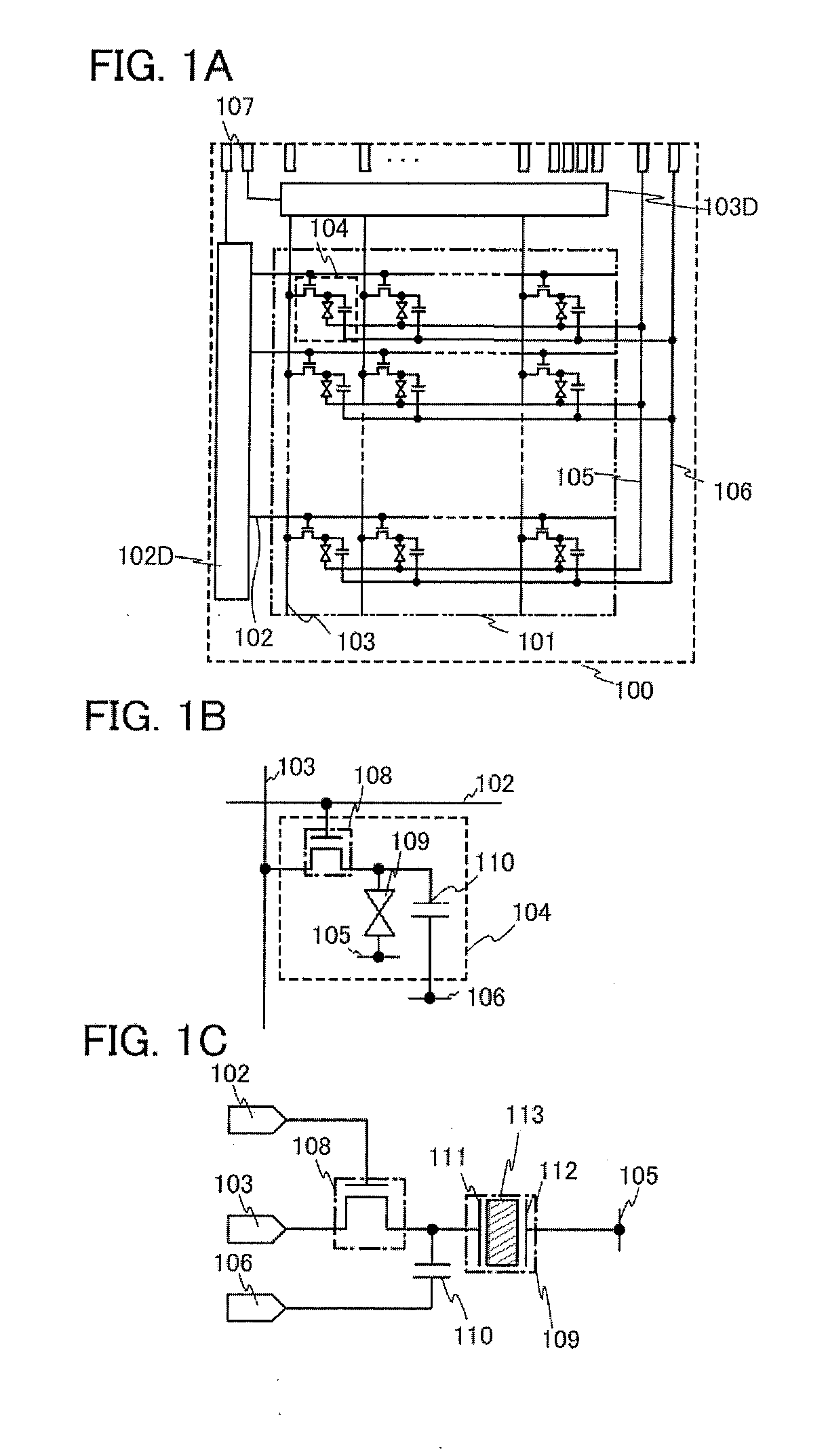
[0039]For explaining this embodiment, FIG. 1A illustrates a schematic diagram of a display panel in a liquid crystal display device. A display panel 100 in FIG. 1A includes a pixel portion 101, a gate line (also referred to as a scan line) 102, a signal line (also referred to as a data line) 103, a pixel 104, a common electrode 105, a capacitor line 106, a terminal portion 107, a gate line driver circuit 102D, and a signal line driver circuit 103D.

[0040]Note that FIG. 1A illustrates the structure in which the gate line driver circuit 102D and the signal line driver circuit 103D are provided over the display panel 100; as in FIG. 14A, the gate line driver circuit 102D and the signal line driver circuit 103D are not necessarily provided over the display panel 100. When the gate line driver circuit 102D and the signal line driver circuit 103D are provided over the display panel 100, the number of terminals in the terminal portion 107 can be reduced and the size of the liquid crystal di...

embodiment 2

[0066]In this embodiment, a structure different from the structure described in Embodiment 1 will be described.

[0067]Embodiment 1 describes the structure for frame inversion driving illustrated in FIG. 6A; this embodiment explains source line inversion driving in which inversion driving with the polarity inverted per signal line is performed as illustrated in FIG. 6B, gate line inversion driving in which inversion driving with the polarity inverted per gate line is performed as illustrated in FIG. 6C, and dot inversion driving in which inversion driving with inverted polarity is performed between adjacent pixels as illustrated in FIG. 6D, by using a circuit configuration of a pixel, and the like. Note that the part of the same description as that in Embodiment 1 is not repeated. Operation for common inversion driving is the same as that for frame inversion driving; therefore, description of common inversion driving is omitted. Note that FIGS. 6A to 6D illustrate examples in which im...

embodiment 3

[0074]In this embodiment, an example of a transistor that can be applied to a liquid crystal display device disclosed in this specification will be described.

[0075]FIGS. 9A to 9D each illustrate an example of a cross-sectional structure of a transistor.

[0076]A transistor 410 illustrated in FIG. 9A is a kind of bottom-gate structure thin film transistor and is also called an inverted staggered thin film transistor.

[0077]The transistor 410 includes, over a substrate 400 having an insulating surface, a gate electrode layer 401, a gate insulating layer 402, an oxide semiconductor layer 403, a source electrode layer 405a, and a drain electrode layer 405b. An insulating layer 407 is provided to cover the transistor 410 and be stacked over the oxide semiconductor layer 403. A protective insulating layer 409 is provided over the insulating layer 407.

[0078]A transistor 420 illustrated in FIG. 9B has a kind of bottom-gate structure called a channel-protective type (channel-stop type) and is a...


PUM


Abstract

An object is to suppress deterioration of a displayed image even when a refresh rate is reduced in displaying a still image. A liquid crystal display device includes a pixel transistor electrically connected to a pixel electrode, and a capacitor having one electrode electrically connected to the pixel electrode and the other electrode electrically connected to a capacitor line. The pixel transistor is turned on and a voltage based on an image signal is supplied to the pixel electrode, and then, the pixel transistor is turned off so that a holding period during which the pixel electrode holds the voltage based on the image signal starts. A holding signal corresponding to change of the voltage based on the image signal in the pixel electrode in the holding period is supplied to the capacitor line so that a potential of the pixel electrode is constant.

Description

TECHNICAL FIELD[0001]The present invention relates to a method for driving a liquid crystal display device, a liquid crystal display device, or an electronic device including a liquid crystal display device.BACKGROUND ART[0002]Liquid crystal display devices are widely used in large display devices such as television sets and small display devices such as mobile phones. Higher value-added devices have been demanded and the development has progressed. In recent years, attention is attracted to the development of low power consumption liquid crystal display devices, in terms of the increase in interest in global environment and improvement in convenience of mobile devices.[0003]Non-Patent Document 1 discloses a structure in which the refresh rate in the case of displaying a moving image and that in the case of displaying a still image are different from each other in order to reduce power consumption of a liquid crystal display device. Moreover, Non-Patent Document 1 discloses a struct...

Claims


Application Information

Patent Timeline
Patent Type & Authority Applications(United States)
IPC IPC(8): G09G5/00
CPCG09G3/3614G09G3/3655G09G2320/10G09G2300/0876G09G2300/0408G09G3/3611G09G2300/0426G02F1/133G09G3/20G09G3/36G02F1/13306G02F1/136213G02F1/1368G09G5/18G09G2300/0404
Inventor MIYAKE, HIROYUKI
Owner SEMICON ENERGY LAB CO LTD
Why Eureka
Try Eureka