Method for driving liquid crystal display device

a liquid crystal display device and display device technology, applied in the direction of instruments, computing, electric digital data processing, etc., can solve the problems of deteriorating images displayed in a period during which image signals are held, power consumption of the liquid crystal display device cannot be reduced sufficiently, and the display of images can be suppressed.

Inactive Publication Date: 2011-06-23
SEMICON ENERGY LAB CO LTD
View PDF101 Cites 76 Cited by
  • Summary
  • Abstract
  • Description
  • Claims
  • Application Information

AI Technical Summary

Benefits of technology

[0009]In view of the above problems, an object of an embodiment of the present invention is to suppress deterioration of images displayed in a liquid crystal display device by reducing the refresh rate in the case of still image display, without complex operation of a driver circuit.
[0015]According to one of the embodiments of the present invention, even if a refresh rate in the case of still image display is decreased, deterioration of displayed images can be suppressed.

Problems solved by technology

When complex driving is performed in a liquid crystal display device as in the structures of Patent Document 1 and Non-Patent Document 1, the structure and operation of a driver circuit which supplies signals to gate lines and signal lines are complicated and thus power consumption of the liquid crystal display device cannot be reduced sufficiently.
However, when the refresh rate in the case of still image display is significantly decreased, images displayed in a period during which image signals are held are deteriorated due to the following problem(s): leakage of charge to be held in a pixel electrode from a pixel transistor and / or disorder of an image signal between a pixel electrode and a common electrode due to noise or the like.

Method used


Image

  • Method for driving liquid crystal display device
  • Method for driving liquid crystal display device
  • Method for driving liquid crystal display device

Examples


embodiment 1

[0032]In this embodiment, block diagrams, timing charts, and the like of liquid crystal display devices will be described.

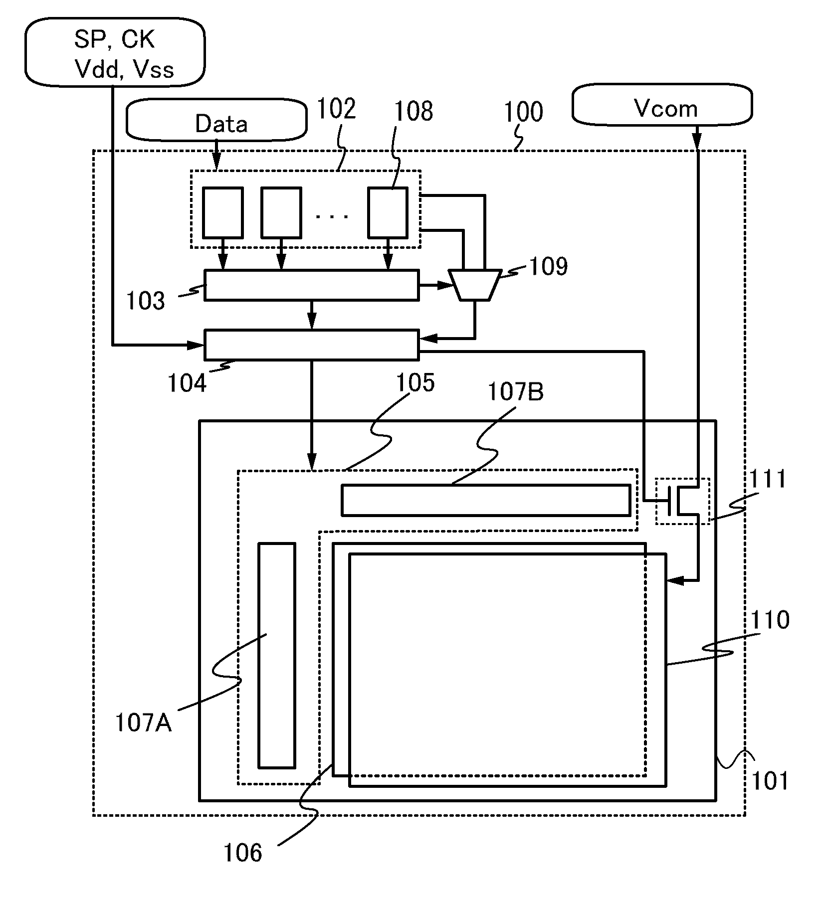
[0033]First, FIG. 1 is a block diagram of a liquid crystal display device, which illustrates components of the liquid crystal display device of this specification.

[0034]A liquid crystal display device 100 in FIG. 1 includes a display panel 101, a memory circuit 102, a comparator circuit 103, a display control circuit 104, and a selection circuit 109.

[0035]The display panel 101 includes, for example, a driver circuit portion 105, a pixel circuit portion 106, a common electrode portion 110, and a switching transistor 111. The driver circuit portion 105 includes a gate line driver circuit 107A and a signal line driver circuit 107B.

[0036]The gate line driver circuit 107A and the signal line driver circuit 107B are driver circuits for driving the pixel circuit portion 106 including a plurality of pixels. The gate line driver circuit 107A and the signal line driver cir...

embodiment 2

[0104]A structure of a display panel in the liquid crystal display device in Embodiment 1 will be described with reference to a specific top view and specific cross-sectional views in FIGS. 7A to 7C.

[0105]FIG. 7A is a top view of a display panel. FIG. 7A is a top view of the display panel in which an FPC has not been attached to a first substrate 1210. FIG. 7B is a cross-sectional view taken along line G-H of FIG. 7A, which illustrates a connection region of a conductive particle and a connection wiring. FIG. 7C is a cross-sectional view taken along line E-F of FIG. 7A, which illustrates a connection region of a pixel circuit and a connection wiring.

[0106]In FIGS. 7A to 7C, the first substrate 1210 which is provided with pixel electrodes and serves as an active matrix substrate and a second substrate 1204 provided with a common electrode 1291 are attached to each other with a sealing material 1205, and the interior space surrounded by the sealing material 1205 is filled with liquid ...

embodiment 3

[0140]In this embodiment, the liquid crystal display device described in the above embodiment, which additionally has a touch panel function, will be described with reference to FIGS. 8A and 8B.

[0141]FIG. 8A is a schematic view of the liquid crystal display device according to this embodiment. FIG. 8A illustrates a structure where a liquid crystal display panel 801 which is the liquid crystal display device according to the above embodiment and a touch panel unit 802 are provided so as to overlap with each other and attached to each other in a housing (case) 803. For the touch panel unit 802, a resistive type, a surface capacitive type, a projected capacitive type, or the like can be used as appropriate.

[0142]As illustrated in FIG. 8A, the liquid crystal display panel 801 and the touch panel unit 802 are separately fabricated and overlapped with each other, whereby the cost for manufacture of the liquid crystal display device additionally having a touch panel function can be reduced...


PUM


Abstract

The liquid crystal display device includes a first substrate provided with a terminal portion, a switching transistor, a driver circuit portion, and a pixel circuit portion including a pixel transistor and a plurality of pixels, a second substrate provided with a common electrode electrically connected to the terminal portion through the switching transistor, and liquid crystal between a pixel electrode and the common electrode. In a period during which a still image is switched to a moving image, the following steps are sequentially performed: a first step of supplying the common potential to the common electrode; a second step of supplying a power supply voltage to the driver circuit portion; a third step of supplying a clock signal to the driver circuit portion; and a fourth step of supplying a start pulse signal to the driver circuit portion.

Description

TECHNICAL FIELD[0001]The present invention relates to a method for driving a liquid crystal display device.BACKGROUND ART[0002]Liquid crystal display devices ranging from a large display device such as a television receiver to a small display device such as a mobile phone have been spreading. From now on, products with higher added values will be needed and are being developed. In recent years, in view of increase in concern about global environment and improvement in convenience of mobile equipment, development of liquid crystal display devices with low power consumption has attracted attention.[0003]Patent Document 1 discloses a structure of a liquid crystal display device where all data signal lines are electrically isolated from a data signal driver, which results in a high impedance state, in order to maintain constant potentials of data signal lines in an idle period during which all gate lines and all the signal lines are not selected. This structure allows reduction in power...

Claims


Application Information

Patent Timeline
Patent Type & Authority Applications(United States)
IPC IPC(8): G06F3/038G09G3/36
CPCG02F1/1345G09G2330/021G09G2320/0219G09G2340/16G09G2320/0209G09G2310/08G09G3/3696G09G2340/0435G09G2320/103G09G2310/04G09G3/3655G09G3/3648G02F1/13306G09G3/36G06F3/044G02F1/13338G06F3/0416G09G3/3618G09G3/3677G09G2320/043G06F3/0421G09G2300/0809G09G2310/061G09G2320/10G09G2354/00
Inventor KOYAMA, JUNMIYAKE, HIROYUKI
Owner SEMICON ENERGY LAB CO LTD
Why Eureka
Try Eureka