Semiconductor integrated circuit including programmable fuse

a technology of integrated circuits and fuses, applied in static storage, digital storage, instruments, etc., can solve the problems of reducing the yield of semiconductor apparatuses, reducing the area of fuse boxes in proportion to the integration density of semiconductor memory apparatuses, and increasing the degree of defect density

Inactive Publication Date: 2011-07-07
SK HYNIX INC
View PDF6 Cites 3 Cited by
  • Summary
  • Abstract
  • Description
  • Claims
  • Application Information

AI Technical Summary

Benefits of technology

[0011]In another aspect of the present invention, a semiconductor integrated circuit comprises: a plurality of fuses each comprising a flash memory element that is programmed to be cut off by a first voltage; and a page buff

Problems solved by technology

As the respective components constituting a semiconductor integrated circuit become smaller, and a greater number of components are integrated into a single semiconductor chip, the degree of defect density also increases.
The increase in the defect density degrades the yield of semico

Method used


Image

  • Semiconductor integrated circuit including programmable fuse
  • Semiconductor integrated circuit including programmable fuse
  • Semiconductor integrated circuit including programmable fuse

Examples


Embodiment Construction

[0017]Hereinafter, a semiconductor integrated circuit including a programmable fuse according to the present invention will be described below with reference to the accompanying drawings through preferred embodiments.

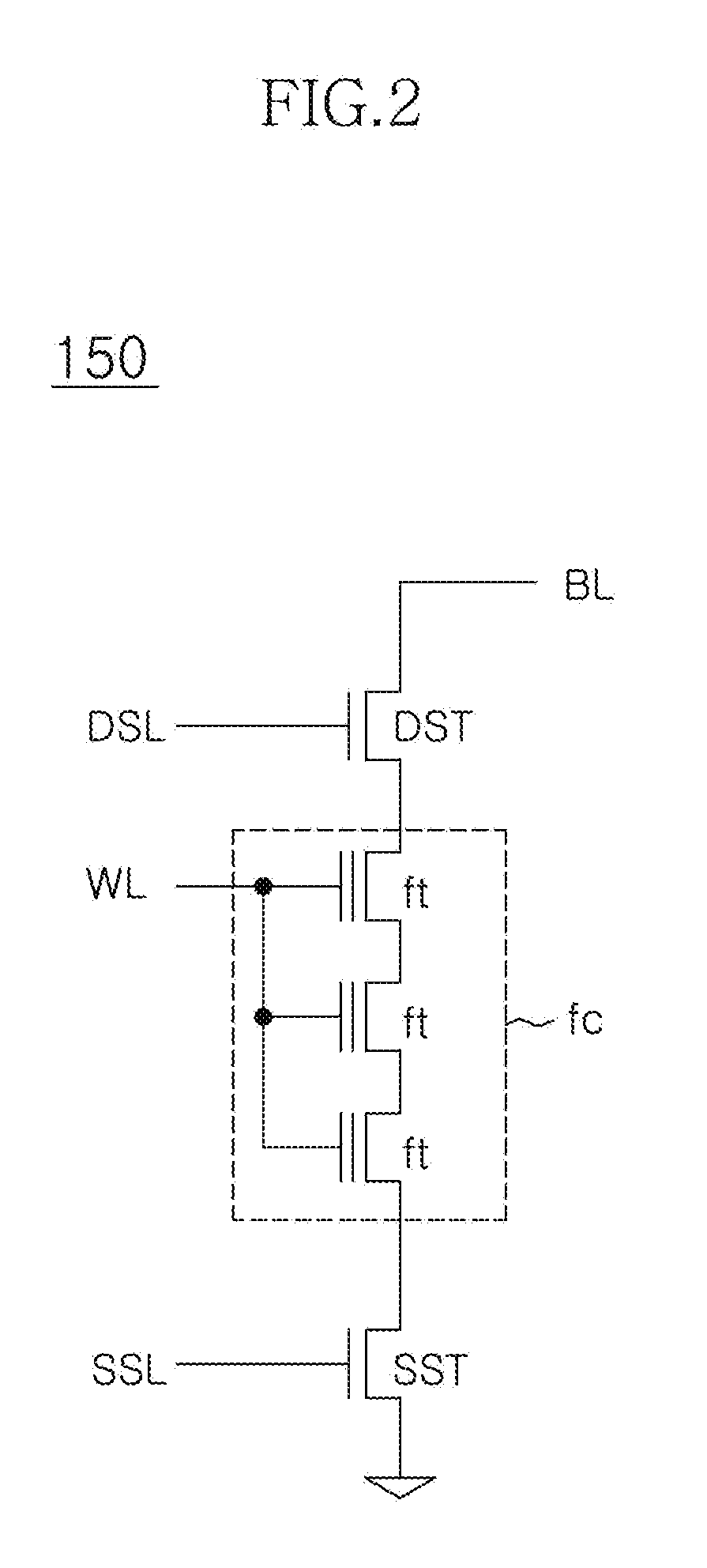
[0018]FIG. 1 is a schematic diagram illustrating a fuse array of a semiconductor integrated circuit according to one embodiment of the invention, and FIG. 2 is a detailed circuit diagram illustrating a fuse of FIG. 1.

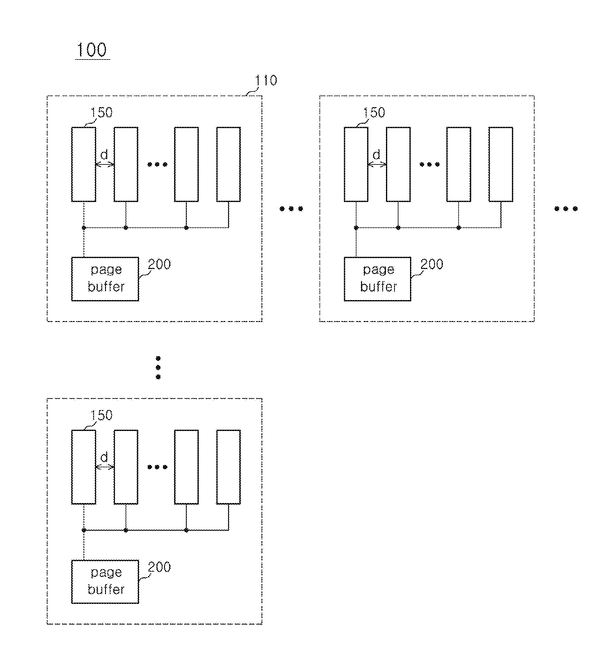
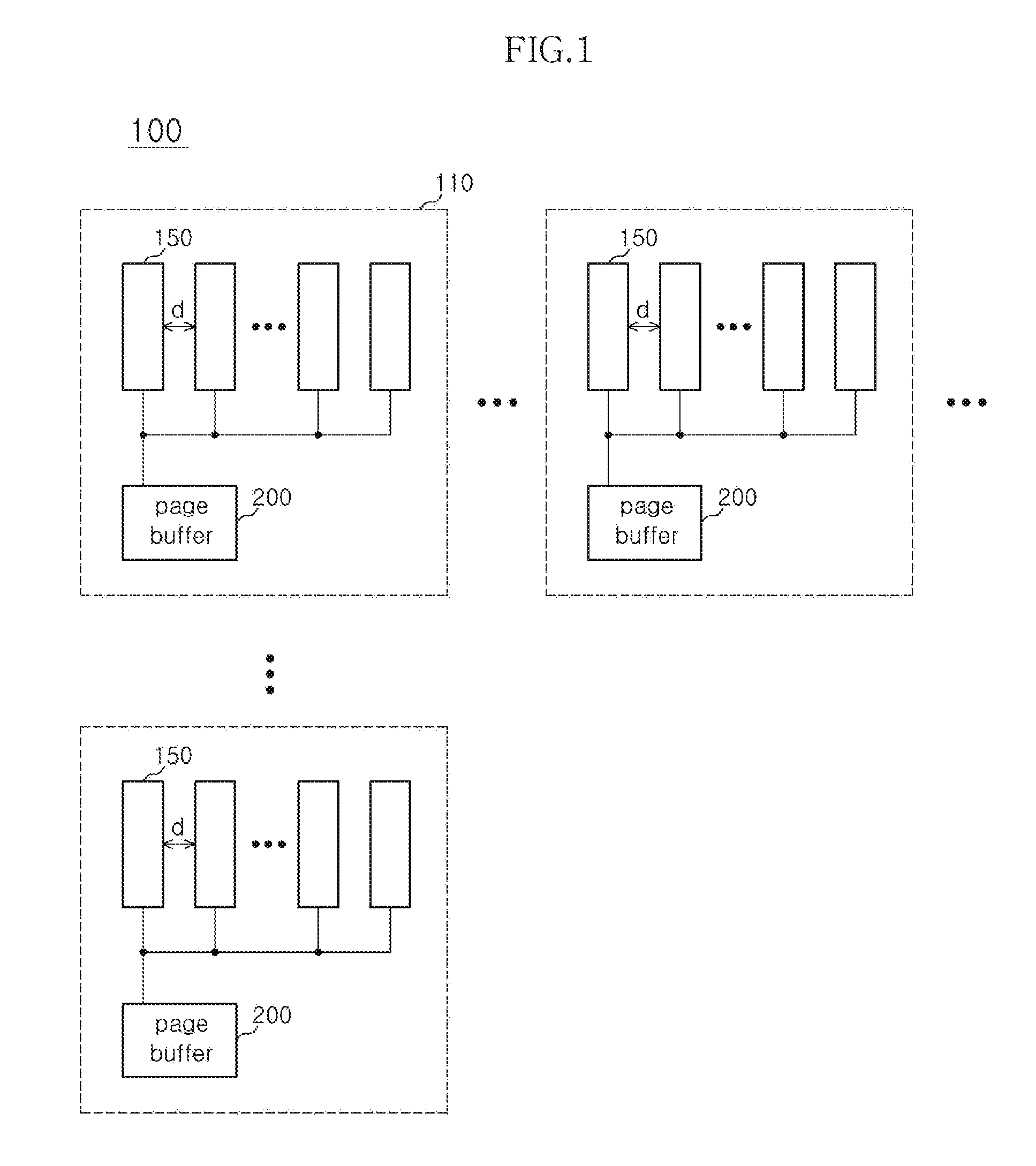
[0019]Referring to FIG. 1, a fuse array 100 comprises a plurality of fuse blocks 110. The plurality of fuse blocks 110 may be arranged in matrix forms.

[0020]The respective fuse blocks 110 may have the same configuration and include a plurality of fuses 150 and a page buffer 200. The respective fuses 150 may be spaced apart by a minimum interval ‘d’ i.e., minimum feature size, which may be provided by a lithography process, regardless of a laser alignment tolerance.

[0021]As illustrated in FIG. 2, each fuse 150 may comprise a single NAND flash string structur...


PUM


Abstract

A semiconductor integrated circuit comprises a plurality of fuses arranged to be spaced apart from one another by predetermined intervals, and a page buffer electrically connected to the plurality of fuses and configured to determine whether to disconnect the fuses. The fuses comprise a NAND flash string. The NAND flash string comprises a drain select transistor connected to a bit line, a flash memory cell electrically connected to the drain select transistor, and a source select transistor connected between the flash memory cell and a ground terminal.

Description

CROSS-REFERENCE TO RELATED APPLICATION[0001]The present application claims priority under 35 U.S.C. §119(a) to Korean Application No. 10-2010-0000431, filed on Jan. 5, 2010, in the Korean Intellectual Property Office, which is incorporated herein by reference in its entirety as if set forth in full.BACKGROUND[0002]1. Technical Field[0003]Various embodiments of the present discloser generally relate to a semiconductor integrated circuit, and more particularly, to a semiconductor integrated circuit including programmable fuses.[0004]2. Related Art[0005]As the respective components constituting a semiconductor integrated circuit become smaller, and a greater number of components are integrated into a single semiconductor chip, the degree of defect density also increases. The increase in the defect density degrades the yield of semiconductor apparatuses. In serious cases, wafers on which semiconductor apparatuses are formed must be discarded.[0006]In order to reduce defect density, redu...

Claims


Application Information

Patent Timeline
IPC IPC(8): G11C16/04G11C17/16
CPCG11C2229/763G11C29/789G11C29/04G11C29/787
Inventor KIM, HONG GYEOMYEON, EUN MI
Owner SK HYNIX INC
Why Eureka
Try Eureka