One-time programmable memory cell, memory and manufacturing method thereof

a one-time programmable memory and memory technology, applied in the direction of transistors, semiconductor/solid-state device details, instruments, etc., can solve the problems of soft breakdown, high power consumption loss, and large power consumption of otp, and achieve the effect of reducing the programming voltag

Inactive Publication Date: 2015-04-28
FUDAN UNIV
View PDF7 Cites 2 Cited by
  • Summary
  • Abstract
  • Description
  • Claims
  • Application Information

AI Technical Summary

Benefits of technology

[0009]The object of the invention is to, in view of the above technical problems, propose an OTP that can be integrated in a back-end structure of integrated circuit and can effectively lower programming voltage.
[0044]The technical effects brought about by the invention can be summarized as follows: in the OTP unit provided by the invention, the storage medium layer is composes of two kinds of metal oxides, and the two kinds of metal oxides are formed by oxidizing different layers of metals that adjoin with each other; therefore, the difference between the two kinds of metal oxides will cause the adjoining area to be easily broken down for programming, thus effectively lowering programming voltage. In addition, the metal oxide layers are formed by performing oxidization on the basis of metal or metal compound. The metal oxide layers can be formed in a back-end structure of integrated circuit, which is totally different from conventional OTP in which the storage medium layer is formed in a front-end structure of integrated circuit; therefore, the thicknesses of the first metal oxide layer and the second metal oxide layer which serve as the storage medium layer can be designed flexibly and determined according to oxidizing conditions (e.g., oxidizing duration). Thus, the process shows great flexibility and the unit area can also be designed smaller. Meanwhile, the preparation method is relatively simple to perform and the cost is low.

Problems solved by technology

High power consumption loss will occur during the breakdown.
Moreover, since the breakdown voltage is high, the power consumption of OTP is relatively large.
Further, with the size of device scaling down proportionally, OTP which is based on oxide layer (i.e., insulating layer) breakdown effect will be subject to the problem of soft breakdown (since the thickness of oxide layer becomes thinner, the probability of occurring soft breakdown is greater).
However, the following problems exist with the OTP unit shown in FIG. 1.
(1) since the OTP is based on gate oxide dielectric layer breakdown and the gate oxide dielectric layer is relatively dense, the breakdown voltage will not be lowered too much; besides, the magnitude of programming voltage mainly depends on the thickness of the gate oxide dielectric layer; therefore, this solution still can not satisfy the requirement of low programming voltage;
(3) when a process node below 32 nm is developed for integrated circuit elements, a high-k dielectric will be commonly used instead of gate oxide dielectric layer; the gate oxide dielectric layer of the OTP unit shown in FIG. 1 will also be replaced by a high-k dielectric layer, which will lead to increase of leakage current, thus increasing power consumption of OTP unit.

Method used


Image

  • One-time programmable memory cell, memory and manufacturing method thereof
  • One-time programmable memory cell, memory and manufacturing method thereof
  • One-time programmable memory cell, memory and manufacturing method thereof

Examples


first embodiment

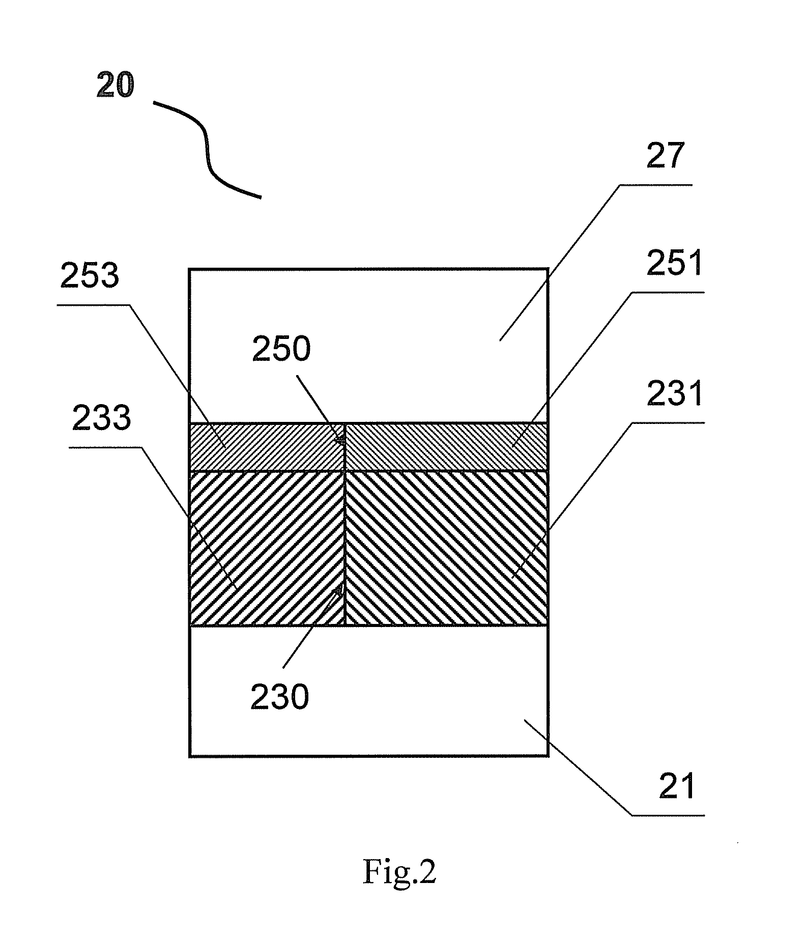
[0056]FIG. 2 is a schematic structural view of an OTP unit in accordance with a first embodiment provided by the invention. In this embodiment, the basic structure of the OTP unit will be described in a simple MIM (metal-insulator-metal) schematic structural view. However, those skilled in the art will appreciate that the OTP unit does not merely comprise the basic structural part shown in FIG. 2. As shown in FIG. 2, the OTP unit 20 also comprises a lower electrode 21 and an upper electrode 27. In this embodiment, a first metal layer 231 and a second metal layer 233 are simultaneously formed on the upper surface of the lower electrode 21. Apparently, the first metal layer 231 and the second metal layer 233 are located in the same layer and adjoin with each other, thus forming the adjoining area 230 shown in the figure. A first metal oxide layer 251 having dielectric characteristic is formed by oxidizing the first metal layer 231, and a second metal oxide layer 253 having dielectric ...

second embodiment

[0062]FIG. 3 is a schematic structural view of an OTP unit in accordance with a second embodiment provided by the invention. Similarly, the OTP unit 30 comprises a lower electrode 21, a first metal layer 331, a second metal layer 333, a first metal oxide layer 351, a second metal oxide layer 353 and an upper electrode 37. An adjoining area 330 exists between the first metal layer 331 and the second metal layer 333, and an adjoining area 350 exists between the first metal oxide layer 351 and the second metal oxide layer 353. The main difference from the OTP unit 20 shown in FIG. 2 lies in that the thicknesses of the first metal oxide layer 351 and the second metal oxide layer 353 that are substantially located in the same layer are different. For example, in this embodiment, the thickness of the second metal oxide layer 353 is smaller than that of the first metal oxide layer 351, and the specific range of thickness difference can be 2-20 nm, e.g., 5 nm, which is not limiting. This is...

third embodiment

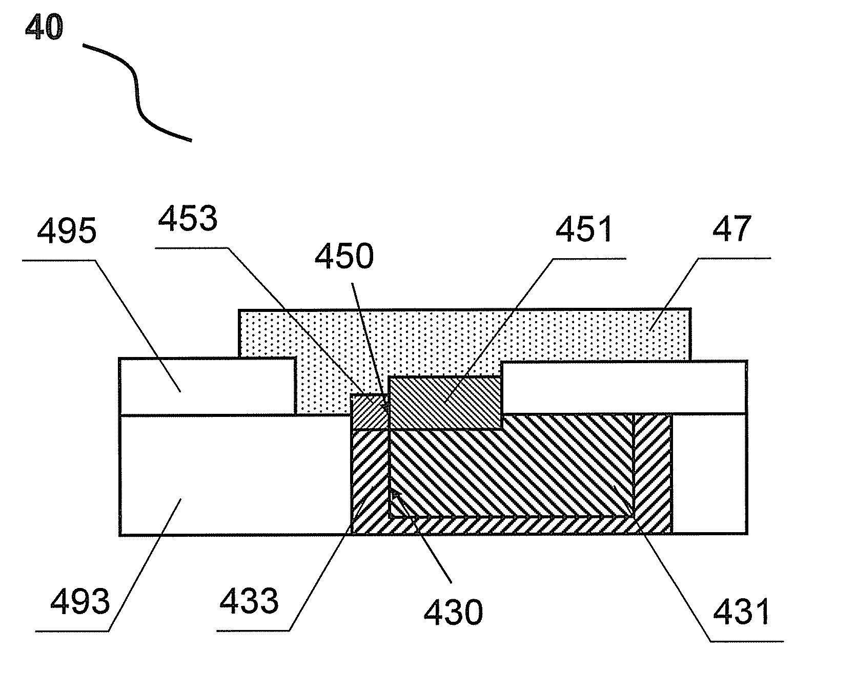
[0063]FIG. 4 is a schematic structural view of an OTP unit in accordance with a third embodiment provided by the invention. Just as described previously, since the OTP unit of the invention is based on metal oxides, it can be formed in a back-end structure of integrated circuit, and the OTP unit 40 of the embodiment shown in FIG. 4 is an OTP unit integrated in the back-end structure. As shown in FIG. 4, the OTP unit 40 also comprises a first metal layer 431, a second metal layer 433, a first metal oxide layer 451, a second metal oxide layer 453, and an upper electrode 47. An adjoining area 430 exists between the first metal layer 431 and the second metal layer 433, and an adjoining area 450 exists between the first metal oxide layer 451 and the second metal oxide layer 453. In this embodiment, the first metal layer 431 and the second metal layer 433 are lead wires in the back-end structure, and the first metal layer 431 and the second metal layer 433 also serve as the lower electrod...


PUM

PropertyMeasurementUnit
thicknessesaaaaaaaaaa
thicknessaaaaaaaaaa

Abstract

The present invention pertains to the technical field of one-time programmable memory (OTP), and in particular to a one-time programmable memory unit, OTP, and method of fabricating the same. The OTP unit comprises a lower electrode, an upper electrode and a storage medium layer placed between the upper electrode and the lower electrode, the storage medium layer comprises a first metal oxide layer and a second metal oxide layer, wherein an adjoining area for programming is formed between the first metal oxide layer and the second metal oxide layer. The OTP comprises a plurality of the above-described one-time programmable memory units arranged in rows and columns. The OTP unit and the OTP have such characteristics as low programming voltage, small unit area, being able to integrate into a back-end structure of integrated circuit, great process flexibility, and the method of fabricating the OTP unit and the OTP is relatively simple and low in cost.

Description

FIELD OF THE INVENTION[0001]The present invention pertains to the technical field of one-time programmable memory (OTP), and in particular relates to a one-time programmable memory unit, OTP, and method of fabricating the same, wherein a storage medium layer is formed using two different layers of metal oxide which are adjacent to each other.BACKGROUND[0002]Non-volatile memories can still preserve the stored data when power is off, which enables them to be widely used in various types of electronic devices. One-time programmable memory (OTP) is one of the commonly used non-volatile memories, which uses memory units having intersected word lines and bit lines to store logic information, wherein a common memory unit has fuse, anti-fuse, and charge capturing devices (e.g., Floating Gate Avalanche-injection Field Effect Transistor). One-time programmable memory is generally non-repeatedly programmable.[0003]For fuse type of OTP and anti-fuse type of OTP, a high voltage is required to br...

Claims


Application Information

Patent Timeline
Patent Type & Authority Patents(United States)
IPC IPC(8): G11C17/16G11C17/00H01L21/768H01L23/525H01L23/538H01L27/112
CPCH01L27/112H01L23/538H01L21/768G11C17/00H01L23/5252H01L27/11206H01L2924/0002H01L2924/00H10B20/00H10B20/20
Inventor LIN, YINYIN
Owner FUDAN UNIV
Why Eureka
Try Eureka