Electric charge capture non-volatile semiconductor storage unit and manufacture method thereof

A technology of charge trapping and manufacturing methods, applied in semiconductor/solid-state device manufacturing, semiconductor devices, electric solid-state devices, etc., which can solve the problems of high power consumption, slow programming speed, and low efficiency of hot electron injection

Inactive Publication Date: 2010-08-11
FUDAN UNIV
View PDF10 Cites 3 Cited by
  • Summary
  • Abstract
  • Description
  • Claims
  • Application Information

AI Technical Summary

Problems solved by technology

In order to generate sufficient hot hole injection at the drain end, the source and drain are both P-N junction structures, which makes it difficult to reduce the programming voltage, low hot electron injection efficiency, slow programming speed, and high power consumption.

Method used


Image

  • Electric charge capture non-volatile semiconductor storage unit and manufacture method thereof
  • Electric charge capture non-volatile semiconductor storage unit and manufacture method thereof
  • Electric charge capture non-volatile semiconductor storage unit and manufacture method thereof

Examples


Embodiment Construction

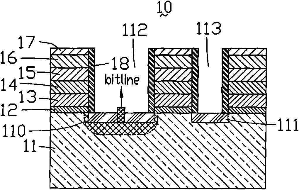
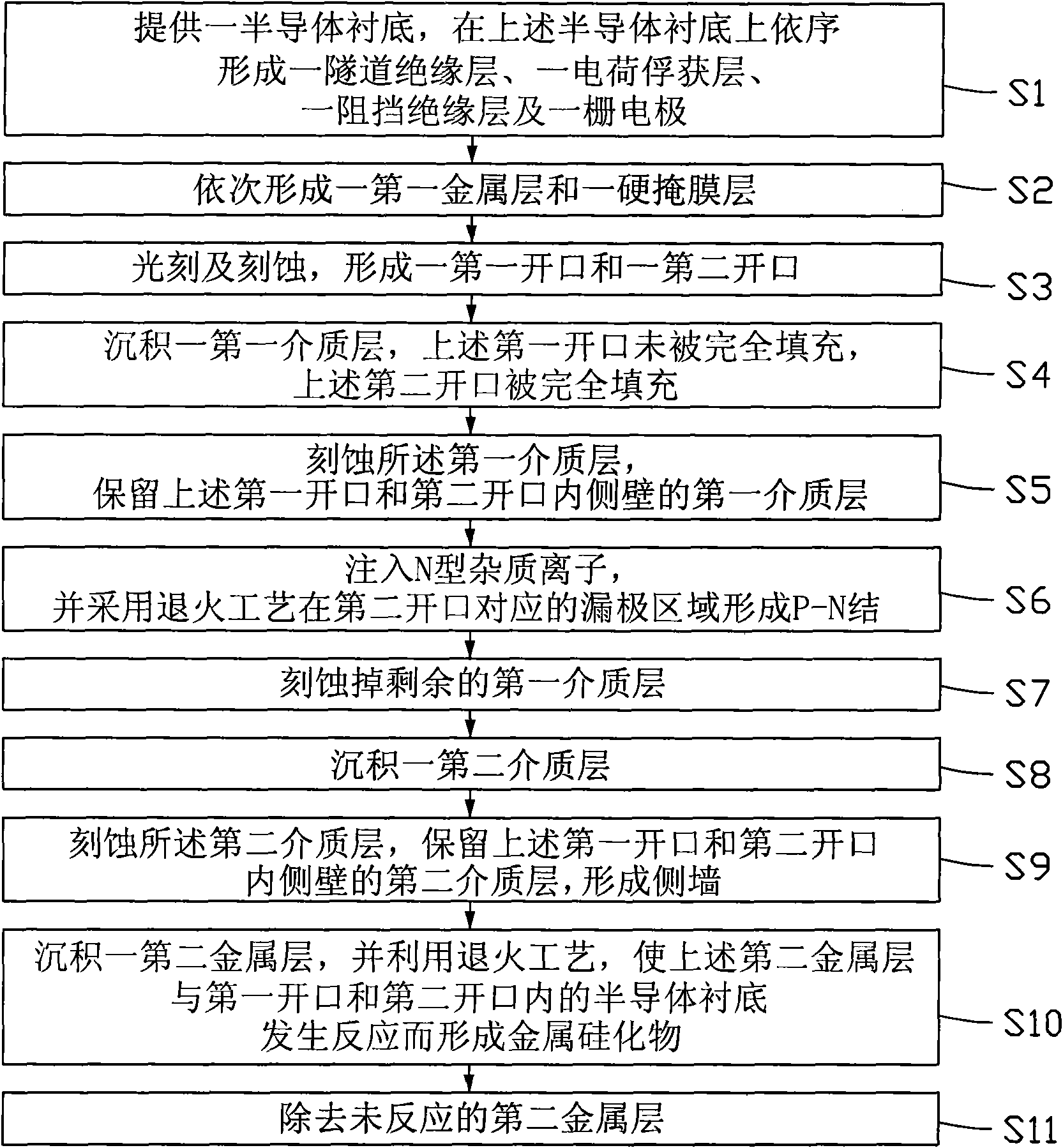
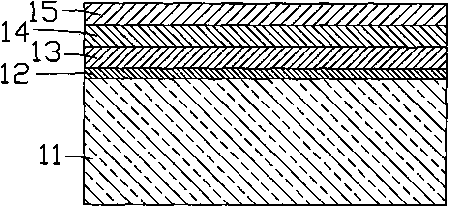
[0026] see figure 1 , figure 1 It is a cross-sectional schematic view of the charge trapping non-volatile semiconductor memory of the present invention. The charge-trapping non-volatile semiconductor memory 10 includes a semiconductor substrate 11, a tunnel insulating layer 12, a charge-trapping layer 13, a blocking insulating layer 14, a gate electrode 15, a first metal layer 16, and a hard mask Layer 17 and side walls 18. The surface of the semiconductor substrate 11 has a drain region 110 and a source region 111 . The above-mentioned tunnel insulating layer 12, charge trapping layer 13, blocking insulating layer 14, gate electrode 15, first metal layer 16 and hard mask layer 17 are sequentially formed on the above-mentioned semiconductor substrate 11 except for the above-mentioned drain region 110 and the above-mentioned source. Areas other than Area 111.

[0027] A first opening 112 and a second opening 113 are respectively formed in spaces corresponding to the drain r...


PUM


Abstract

The invention provides an electric charge capture non-volatile semiconductor storage unit and a manufacture method thereof. The electric charge capture non-volatile semiconductor storage unit comprises a semiconductor substrate, a source region, a drain region and a tunnel insulating layer, and an electric charge capture layer, a barrier insulating layer and a gate electrode layer which are formed on the semiconductor substrate in sequence, wherein the drain region comprises a P-N junction, and the source region comprises a metal semiconductor junction formed by any one of titanium, cobalt, nickel and platinum or a mixture thereof with the semiconductor substrate. The electric charge capture non-volatile semiconductor storage unit has low programming voltage, low programming speed, lower power consumption and higher reliability.

Description

technical field [0001] The invention relates to a non-volatile memory, in particular to a charge-trapping non-volatile semiconductor memory and a preparation method thereof. Background technique [0002] Non-volatile memory (Non-volatile memory) has a wide range of applications in the fields of mobile communications, data terminals, multimedia, consumer electronics, and defense electronic equipment due to its low power consumption, small size, high density, and rewritable characteristics. . [0003] The non-volatile memory mainly includes floating gate (Floating Gate) non-volatile semiconductor memory and charge trapping (Charge Trapping) non-volatile semiconductor memory. The floating gate non-volatile semiconductor memory uses polysilicon to form a floating gate, and charges are stored in the floating gate, so if there are any defects in the above-mentioned polysilicon, the charge retention time will be significantly reduced. In contrast, the charge-trapping non-volatile...

Claims


Application Information

Patent Timeline
Patent Type & Authority Applications(China)
IPC IPC(8): H01L29/792H01L21/336
CPCH01L27/11521H01L29/792H01L27/11568H10B43/30H10B41/30
Inventor 吴东平张世理
Owner FUDAN UNIV
Why Eureka
Try Eureka