High speed nano two-end nonvolatile storage and manufacturing method thereof

A non-volatile memory technology, applied in nanotechnology, nanotechnology, nanotechnology for information processing, etc., can solve the problem of large size, long read/write time and preparation process of nano field effect tube memory, difficult threshold Problems such as voltage drift, to improve the effect of large memory size, fast read/write speed, and simple preparation method

Active Publication Date: 2014-05-28
合肥庐阳科技创新集团有限公司
View PDF3 Cites 3 Cited by
  • Summary
  • Abstract
  • Description
  • Claims
  • Application Information

AI Technical Summary

Problems solved by technology

Due to the large size of the nano-FET memory, it is difficult to control the threshold voltage drift, the high programming voltage, the long read / write time, and the preparation process is complicated and difficult to repeat, which seriously hinders its application.

Method used


Image

  • High speed nano two-end nonvolatile storage and manufacturing method thereof
  • High speed nano two-end nonvolatile storage and manufacturing method thereof
  • High speed nano two-end nonvolatile storage and manufacturing method thereof

Examples


Embodiment 1

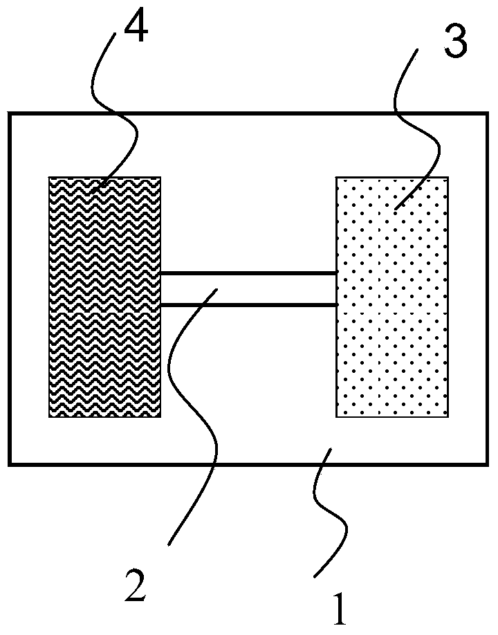
[0031] In this embodiment, Cu-doped p-type ZnS nanobelts are used as p-type doped one-dimensional nanomaterials 2, Cu electrodes are used as metal electrodes 4, and silicon wafers with a thickness of 300 nm on the surface are used as insulating substrates. 1. A p-type ZnS nanoribbon / Cu electrode high-speed non-volatile memory with both ends was prepared. The specific steps are as follows:

[0032] (1) At room temperature, after ultrasonically cleaning the silicon wafer with a thickness of 300nm on the surface of silicon oxide, alcohol is used as the dispersion liquid, and the p-type doped ZnS nanoribbons synthesized by chemical vapor phase are added to the dispersion liquid, and the nanobelts are ultrasonically oscillated. The ribbon is evenly suspended in the dispersion; and the dispersion containing the ZnS nanoribbon is spin-coated on a clean long silicon wafer with a silicon oxide layer;

[0033] (2) Spin-coat photoresist on the silicon wafer coated with ZnS nanoribbons, a...

Embodiment 2

[0039] In this example, p-type ZnS nanobelts were prepared by using Ag-doped p-type ZnS nanobelts as p-type doped one-dimensional nanomaterials 2, using Ag electrodes as metal electrodes 4, and using quartz glass as insulating substrate 1. / Ag electrode high-speed non-volatile memory at both ends, the specific steps are as follows:

[0040] (1) At room temperature, after the quartz glass is ultrasonically cleaned, alcohol is used as a dispersion liquid, and p-type doped ZnS nanobelts synthesized by chemical vapor phase are added to the dispersion liquid, and the nanobelts are evenly suspended in the dispersion liquid by ultrasonic vibration; and Spin-coat the dispersion containing ZnS nanobelts on clean quartz glass;

[0041] (2) Spin-coat photoresist on the silicon wafer coated with ZnS nanoribbons, and photoetch the electrode pattern of the metal electrode 4;

[0042](3) A layer of Ag electrode is prepared in the electrode pattern area of ​​the photolithographic metal elect...

Embodiment 3

[0047] In this embodiment, the Ag-doped p-type ZnSe nanobelt is used as the p-type doped one-dimensional nanomaterial 2, the Cu electrode is used as the metal electrode 4, and the silicon wafer with a thickness of 300 nm on the surface is used as the insulating substrate. Bottom 1, a p-type ZnSe nanoribbon / Cu electrode high-speed non-volatile memory with both ends was prepared. The specific steps are as follows:

[0048] (1) At room temperature, after ultrasonically cleaning the silicon wafer with a thickness of 300nm on the surface of silicon nitride, alcohol was used as the dispersion liquid, and the p-type doped ZnSe nanoribbons synthesized by chemical vapor phase were added to the dispersion liquid, and ultrasonic vibration was used to make Nanobelts are uniformly suspended in the dispersion; and the dispersion containing ZnSe nanobelts is spin-coated on a clean silicon wafer with silicon oxide;

[0049] (2) Spin-coat photoresist on the silicon wafer coated with ZnSe nanor...


PUM

PropertyMeasurementUnit
thicknessaaaaaaaaaa
thicknessaaaaaaaaaa
thicknessaaaaaaaaaa

Abstract

The invention discloses a high speed nano two-end nonvolatile storage and a manufacturing method thereof. The high speed nano two-end nonvolatile storage is characterized in that p-type doping one-dimensional nanomaterials, a graphene electrode and a metal electrode are distributed on an insulating substrate, and the graphene electrode is communicated with the metal electrode through the p-type doping one-dimensional nanomaterials; the p-type doping one-dimensional nanomaterials are p-type doping ZnS one-dimensional nanomaterials or p-type doping ZnSe one-dimensional nanomaterials; the metal electrode is a Cu electrode or a Ag electrode. The manufacturing method of the high speed nano two-end nonvolatile storage is simple, easy to control, high in rate of finished products and capable of being applied to large-scale integration conveniently. The manufactured storage has the excellent characteristics of being low in programming voltage, high in reading / writing speed, long in retention time and the like, thereby having a potential application prospect in development of a low-power dissipation, high speed and high integration density storage.

Description

technical field [0001] The invention belongs to the technical field of semiconductor devices, and in particular relates to a high-speed nano-terminal nonvolatile memory and a preparation method thereof. Background technique [0002] Semiconductor memory is an important branch field in the research of microelectronics. It plays the function of storing and processing information and is widely used in various microelectronic devices. Among them, non-volatile memory plays an increasingly important role in the semiconductor industry and plays a major role. With the rapid development of digital high-tech, higher requirements are placed on the performance of memory, such as high speed, high density, low power consumption, long life and smaller size. Especially when the feature size of the device is reduced, the contradiction between the reading and writing speed and reliability of the traditional floating gate memory device and the leakage of the gate dielectric limit the further ...

Claims


Application Information

Patent Timeline
Patent Type & Authority Applications(China)
IPC IPC(8): H01L45/00B82Y10/00
Inventor 于永强蒋阳郑坤王莉吴春艳朱志峰
Owner 合肥庐阳科技创新集团有限公司
Why Eureka
Try Eureka