
Method of forming circuit interconnection, circuit board, and circuit interconnection film having film thickness larger than width thereof

a technology of circuit interconnection and film thickness, which is applied in the direction of resistive material coating, railway components, nuclear engineering, etc., can solve the problems of affecting the uniformity of the film thickness of the circuit interconnection film that forms the circuit interconnection, the inability to make the width of the circuit interconnection smaller than a predetermined width, and the substantial removal of the possibility of the circuit interconnection film becoming non-uniform

Inactive Publication Date: 2011-07-21
SEIKO EPSON CORP
View PDF6 Cites 0 Cited by
  • Summary
  • Abstract
  • Description
  • Claims
  • Application Information

AI Technical Summary

Benefits of technology

The invention provides a method for forming a circuit interconnection on a circuit board by depositing a metal film using a catalyst for forming the conductive layer. The method includes a trench forming process and a catalyst distribution process. The method allows for the formation of a uniform circuit interconnection film with a fine pattern width, and also allows for the easy removal of smear inside the trench. The method can be performed using a laser process for forming the trench, which allows for precise formation of the trench. The method can also include a desmear processing process to remove smear from the circuit interconnection film. The functional solution containing the catalyst for forming the conductive layer can be distributed on the base material surface using an ink jet type discharge device, which allows for precise distribution on a fine trench. The method can also include distributing the functional solution on a portion having a wide width of the trench using capillary force. Overall, the method provides a simple and effective solution for forming circuit interconnections on circuit boards.

Problems solved by technology

However, according to the method as disclosed in JP-A-2005-12181, if the functional solution containing metal flows into the circuit interconnection forming area, there is a possibility that the functional solution is not sufficiently filled into a portion having a narrow width of the circuit interconnection forming area due to the unevenness of the flow distribution, and thus the film thickness of the circuit interconnection film that forms the circuit interconnection is liable to become non-uniform.
According to the method as disclosed in JP-A-2009-117415, it is impossible to make the width of a circuit interconnection smaller than a predetermined width due to the fact that the width of the circuit interconnection is unable to be smaller than the width of the interconnection of the circuit pattern initially formed.
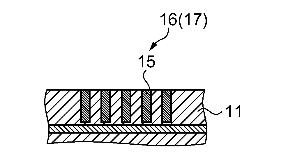
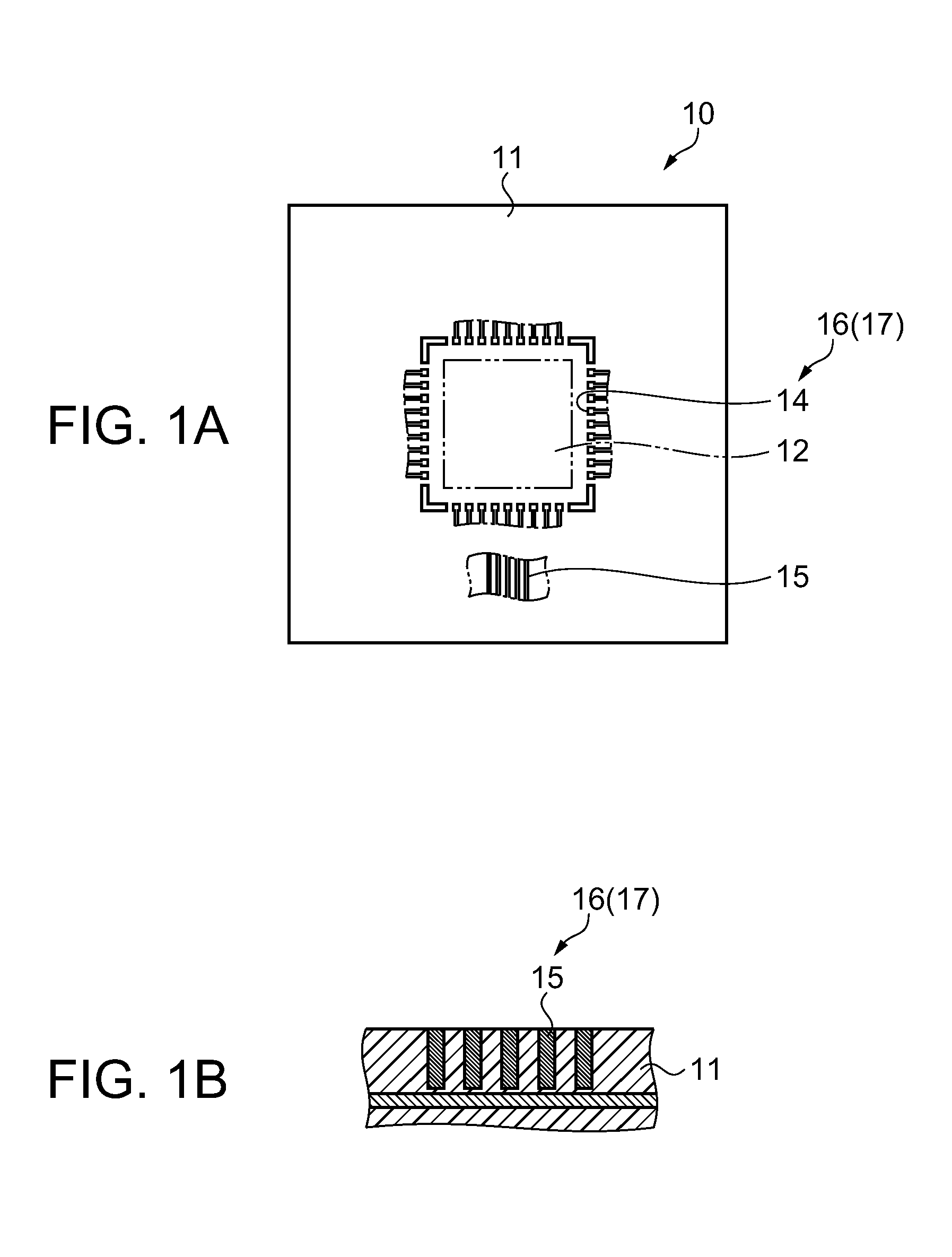
Also, since the conductive material is deposited by plating such as electroless plating, the possibility is substantially removed of the circuit interconnection film that forms the circuit interconnection becoming non-uniform, and thus a uniform circuit interconnection can be formed.
Also, since the conductive material is deposited by plating such as electroless plating, the possibility is substantially removed of the circuit interconnection film becoming non-uniform.

Method used


Image

  • Method of forming circuit interconnection, circuit board, and circuit interconnection film having film thickness larger than width thereof
  • Method of forming circuit interconnection, circuit board, and circuit interconnection film having film thickness larger than width thereof
  • Method of forming circuit interconnection, circuit board, and circuit interconnection film having film thickness larger than width thereof

Examples


modified example 1

[0083]In the above-described embodiment, the plating process of the circuit interconnection forming process has the electroless plating process and the electro plating process, but it is not essential to perform the electro plating process together with the electroless plating process. The circuit interconnection forming method may be a method of forming the circuit interconnection film only by the electroless plating process.

modified example 2

[0084]In the above-described embodiment, the catalyst functional solution 31 is distributed on the trench 21A using the ink jet type droplet discharge apparatus, but it is not essential to use the ink jet type droplet discharge apparatus to distribute the functional solution that includes the catalyst for forming the conductive layer. Any droplet discharge apparatus that is different from the ink jet type droplet discharge apparatus may be used, and the functional solution may be distributed using another apparatus that is different from the droplet discharge apparatus.

modified example 3

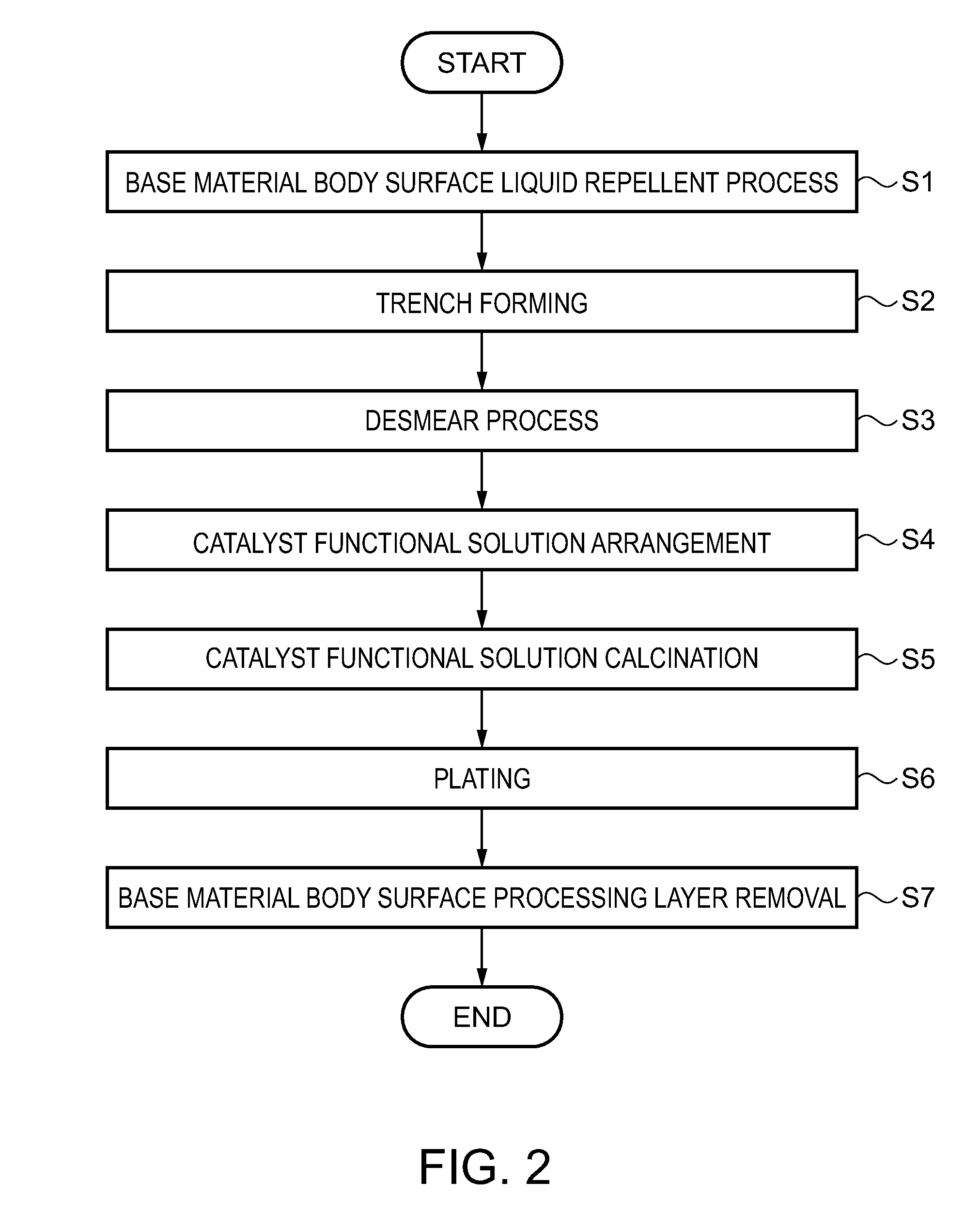
[0085]In the above-described embodiment, in the process of forming the circuit interconnection, a desmear process including a cleaning process, a smear removing process, a neutralization process, and a cleaning process is performed. However, performing of the desmear process is not essential. If it is possible to suppress the occurrence of smear when the trench is formed, the process of forming the circuit interconnection may be a process that does not include the desmear process.


PUM

PropertyMeasurementUnit
thickness aspect ratioaaaaaaaaaa
invading distanceaaaaaaaaaa
temperatureaaaaaaaaaa

Abstract

A method of forming a circuit interconnection on a circuit board includes: forming a trench that corresponds to a shape of the circuit interconnection on an interconnection base material that forms the circuit interconnection; distributing a catalyst for forming a conductive layer on the trench; and forming a conductive circuit interconnection film that forms the circuit interconnection by distributing a plating solution in a range that includes the trench and depositing a conductive material from the plating solution through the catalyst for forming the conductive layer.

Description

BACKGROUND[0001]1. Technical Field[0002]The present invention relates to a method of forming a circuit interconnection on a circuit board, a circuit board formed using the method of forming a circuit interconnection, and a circuit interconnection film which is formed using the corresponding method of forming a circuit interconnection and has a film thickness that is greater than a width thereof.[0003]2. Related Art[0004]Up until now, semiconductor devices have been packaged and used on circuit boards. Recently, with the remarkable development of high-performance miniaturized semiconductor devices, miniaturized high-performance circuit boards for mounting the semiconductor device have also come into demand. In order to achieve miniaturized circuit boards, miniaturized high-density circuit interconnections that form the circuit boards are necessary. In order to make high-performance circuit boards, low resistance circuit interconnections (which have a large cross-sectional area and no...

Claims


Application Information

Patent Timeline
Patent Type & Authority Applications(United States)
IPC IPC(8): H05K1/11H01B5/00H05K3/12
CPCH05K3/181H05K3/107
Inventor KAMAKURA, TOMOYUKI
Owner SEIKO EPSON CORP
Learn More