Touch display panel
a display panel and touch technology, applied in the field of touch display panels, can solve the problems of increasing the thickness of the display panel, complicating the fabrication process of the touch display panel, and further complicating the fabrication process, so as to achieve the effect of simple fabrication process and simple structur
- Summary
- Abstract
- Description
- Claims
- Application Information
AI Technical Summary
Benefits of technology
Problems solved by technology
Method used
Image

Examples
first embodiment
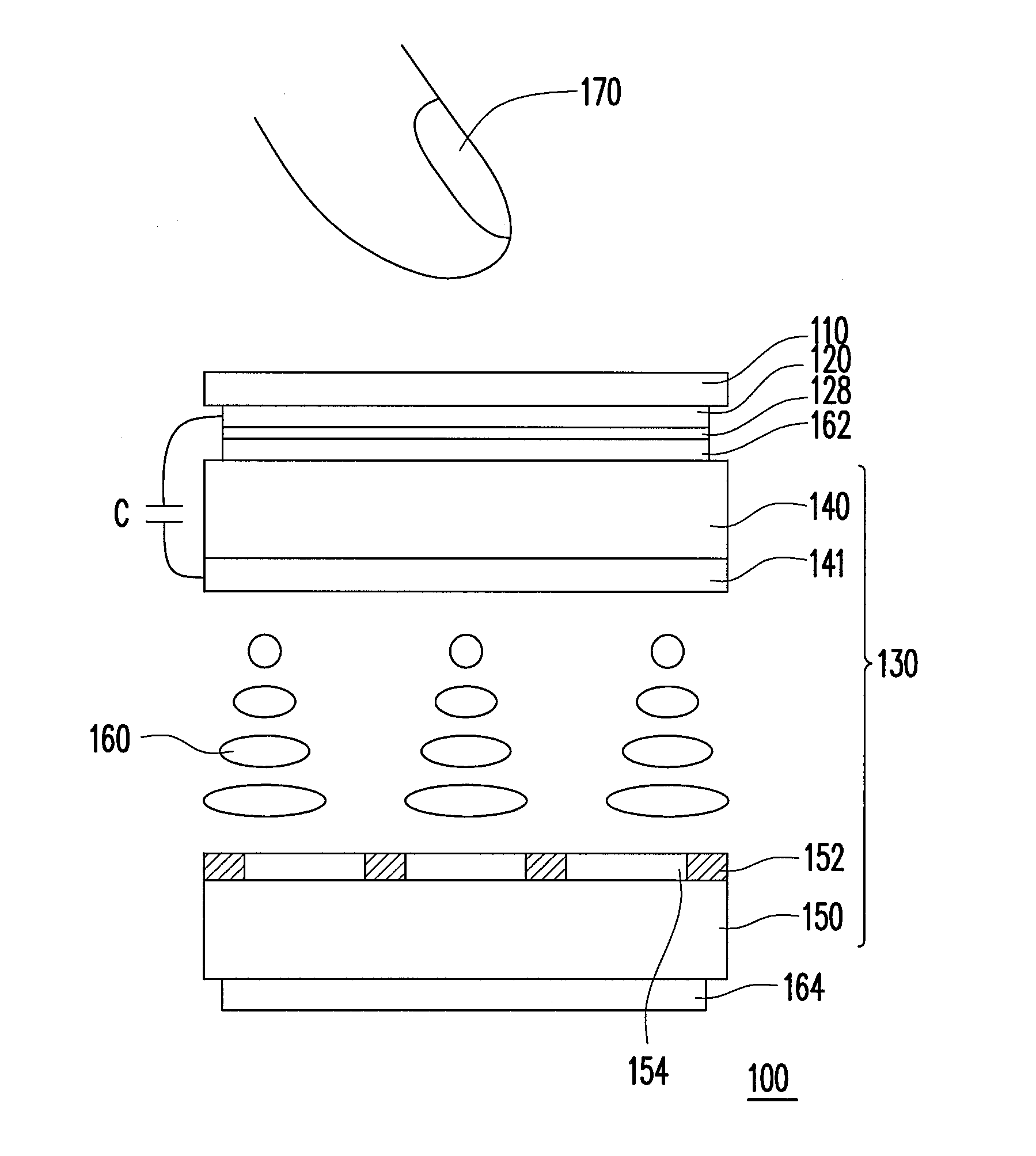
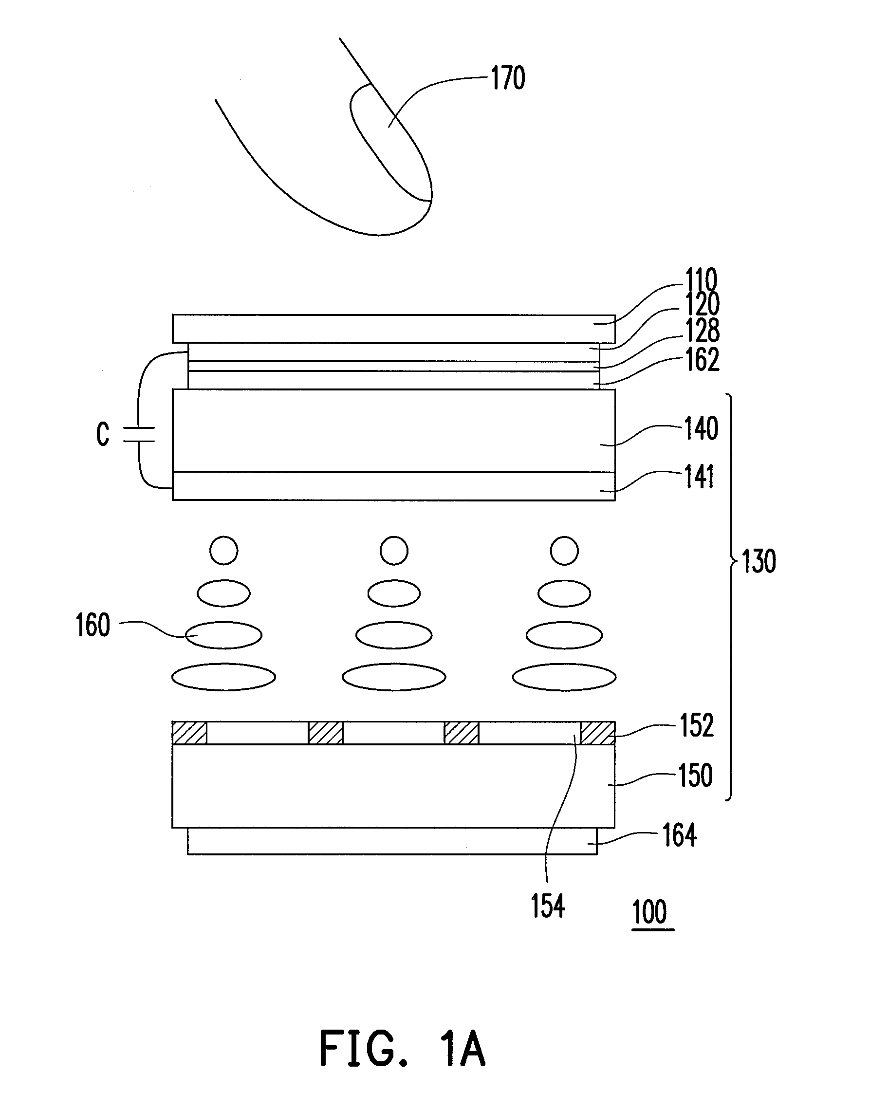
[0020]Referring to FIG. 1A and FIG. 1B, a touch display panel 100 includes a cover plate 110, a plurality of touch sensing electrodes 120, an adhesion layer 128 and a display panel 130.
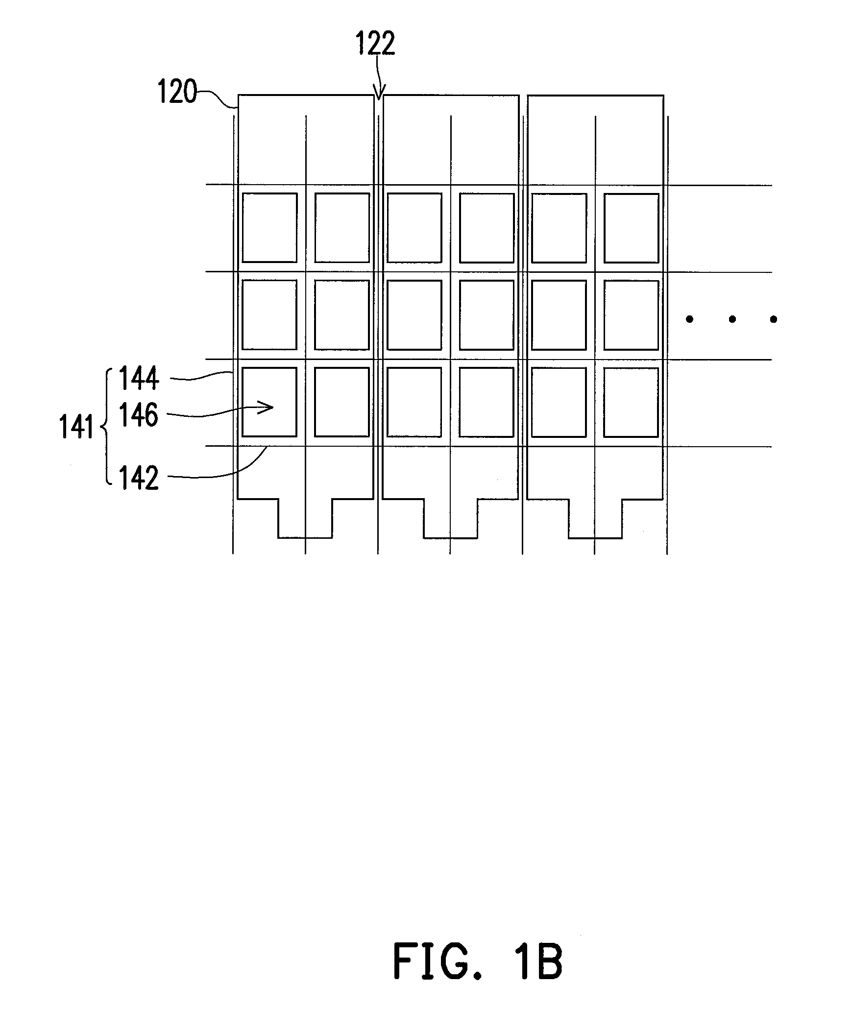
[0021]The display panel 130 includes a substrate 140, an opposite substrate 150 and a display medium layer 160, wherein the opposite substrate 150 is parallel to the substrate 140. The display medium layer 160 is disposed between the substrate 140 and the opposite substrate 150. The substrate 140 is a pixel array substrate, and a pixel array 141 is disposed thereon. The pixel array 141 includes a plurality of scan lines 142, a plurality of data lines 144 and a plurality of pixel structures 146. Each of the pixel structures 146 is electrically connected to one of the scan lines 142 and one of the data lines 144, and the scan lines 142 are not parallel to the data lines 144. The data lines 144 are disposed at a side of the substrate 140 different to a side where the touch sensing electrodes 120 are loca...
second embodiment
[0026]Referring to FIG. 2A and FIG. 2B, the touch display panel 200 includes a cover plate 210, a plurality of touch sensing electrodes 220, an adhesion layer 228 and a display panel 230.
[0027]The display panel 230 includes a substrate 240, a plurality of scan lines 242, an opposite substrate 250 and a display medium layer 260, wherein the opposite substrate 250 is parallel to the substrate 240. The touch sensing electrodes 220 are disposed between the cover plate 210 and the substrate 240. The scan lines 242 are disposed on the substrate 240, and the display medium layer 260 is disposed between the substrate 240 and the opposite substrate 250. A sensing capacitance C is formed between the touch sensing electrodes 220 and the scan lines 242, and when a conductive object 270 approaches the cover plate 210, a position of the conductive object 270 can be calculated according to a variation of the sensing capacitance C.
[0028]Referring to FIG. 2B and FIG. 2C, in the present embodiment, t...
PUM
 Abstract
Description
Claims
Application Information
 - Generate Ideas
- Intellectual Property
- Life Sciences
- Materials
- Tech Scout
- Unparalleled Data Quality
- Higher Quality Content
- 60% Fewer Hallucinations
Browse by: Latest US Patents, China's latest patents, Technical Efficacy Thesaurus, Application Domain, Technology Topic, Popular Technical Reports.
© 2025 PatSnap. All rights reserved.Legal|Privacy policy|Modern Slavery Act Transparency Statement|Sitemap|About US| Contact US: help@patsnap.com