
Image Sensor Devices Having Peripheral Circuits Therein that Use Light Guide Materials as Electrical Insulators

a technology of image sensor and peripheral circuit, which is applied in the direction of color television, basic electric elements, television systems, etc., can solve problems such as reliability problems of image sensors

Active Publication Date: 2011-07-21
SAMSUNG ELECTRONICS CO LTD
View PDF3 Cites 17 Cited by
  • Summary
  • Abstract
  • Description
  • Claims
  • Application Information

AI Technical Summary

Problems solved by technology

However, in the case of an image sensor formed through such a manufacturing process, faults such as cracks or the like occur on the optical guide part spread on a conductive pad, and this causes problems in reliability of the image sensor.

Method used


Image

  • Image Sensor Devices Having Peripheral Circuits Therein that Use Light Guide Materials as Electrical Insulators
  • Image Sensor Devices Having Peripheral Circuits Therein that Use Light Guide Materials as Electrical Insulators
  • Image Sensor Devices Having Peripheral Circuits Therein that Use Light Guide Materials as Electrical Insulators

Examples


Embodiment Construction

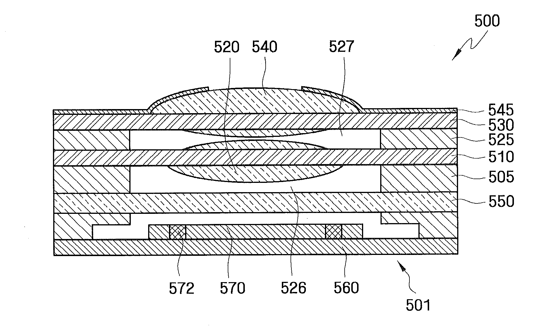
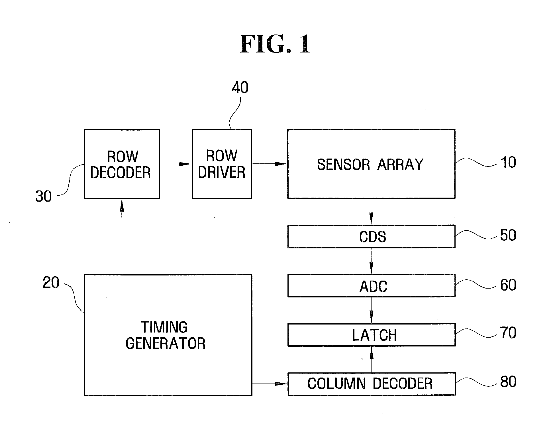
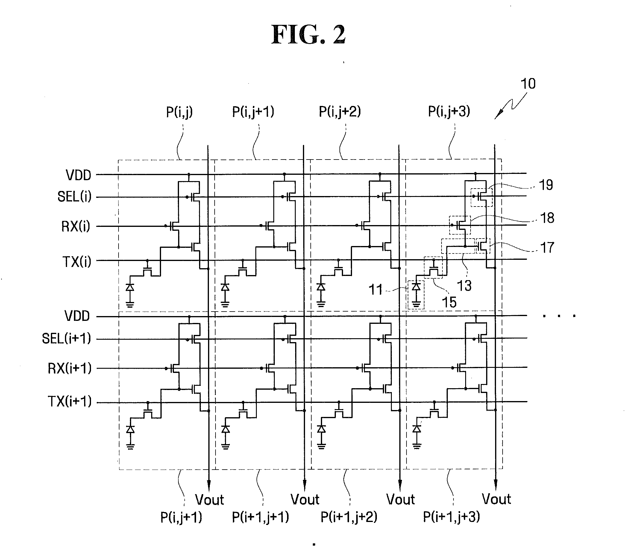
Hereinafter, preferred embodiments of the present invention will be described in detail with reference to the accompanying drawings. The aspects and features of the present invention and methods for achieving the aspects and features will be apparent by referring to the embodiments to be described in detail with reference to the accompanying drawings. However, the present invention is not limited to the embodiments disclosed hereinafter, but can be implemented in diverse forms. The matters defined in the description, such as the detailed construction and elements, are nothing but specific details provided to assist those of ordinary skill in the art in a comprehensive understanding of the invention, and the present invention is only defined within the scope of the appended claims. In some embodiments of the present invention, well-known element structures and technologies are not described in detail since they would obscure the invention in unnecessary detail.

Although the terms “fir...


PUM


Abstract

An image sensor includes an array of image sensor cells, on a substrate, and a peripheral circuit region extending adjacent the array of image sensor cells. The array of image sensor cells includes a plurality of lens elements and a plurality of color filters extending adjacent the plurality of lens elements. A plurality of photodiodes is provided in the substrate. The plurality of photodiodes are aligned to corresponding ones of the plurality of lens elements. An interconnection structure is also provided, which extends between the plurality of photodiodes and the plurality of color filters. The interconnection structure has an array of cavities therein that are aligned to corresponding ones of the plurality of photodiodes and are filled with a light guide material. The peripheral circuit region includes a metal interconnect pattern and an electrically conductive pad on the metal interconnect pattern. An electrically insulating layer extends on the electrically conductive pad. The electrically insulating layer is formed of the light guide material.

Description

REFERENCE TO PRIORITY APPLICATIONThis application claims priority to Korean Patent Application No. 10-2010-0005703, filed Jan. 21, 2010, the contents of which are hereby incorporated herein by reference.FIELDThe present invention relates to image sensors and imaging devices including the image sensor.BACKGROUNDAn image sensor is a sensor that converts an optical image into an electric signal. Recently, with the development of computer industry and communications industry, there is an increasing demand for image sensors having improved performance in diverse fields including a digital camera, a camcorder, a PCS (Personal Communication System), a game machine, a guard camera, a micro camera for medical use, and the like.In particular, a MOS image sensor has a simple drive system and adopts diverse scanning methods. Also, its signal processing circuit can be integrated into one chip to facilitate the miniaturization of the product, and the MOS processing technology can be compatibly us...

Claims


Application Information

Patent Timeline
Patent Type & Authority Applications(United States)
IPC IPC(8): H04N5/228H04N23/40
CPCH04N5/374H01L27/14618H01L27/14627H04N5/2257H01L27/14632H01L27/14636H01L27/14629H01L2924/0002H04N23/57H04N25/76H01L2924/00H01L23/564
Inventor CHO, JUNG-HYUNLEE, JUNE-TAEGHEO, SUN-WOOKCHUN, KEE-MOON
Owner SAMSUNG ELECTRONICS CO LTD
Features
  • Generate Ideas
  • Intellectual Property
  • Life Sciences
  • Materials
  • Tech Scout
  • Unparalleled Data Quality
  • Higher Quality Content
  • 60% Fewer Hallucinations
Learn More