
Method for forming pattern and a wired board

a wired board and pattern technology, applied in the direction of conductive pattern formation, printed circuit aspects, printed circuit manufacturing, etc., can solve the problems of large equipment, high production cost, and certain limits, and achieve the effect of fine conductive patterns and easy forming of patterns

Active Publication Date: 2011-08-04
BROTHER KOGYO KK
View PDF13 Cites 8 Cited by
  • Summary
  • Abstract
  • Description
  • Claims
  • Application Information

AI Technical Summary

Benefits of technology

This method allows for the easy formation of patterns with fine widths and reduced production costs by charging conductive liquid into narrow grooves, enhancing the reliability and density of conductive patterns on base materials, and facilitating the connection of electronic components without damaging them.

Problems solved by technology

Therefore, the apparatus or equipment is large-sized, and the production cost is expensive as well.
Therefore, there is a certain limit even when it is intended to decrease the width of the conductive pattern.

Method used


Image

  • Method for forming pattern and a wired board
  • Method for forming pattern and a wired board
  • Method for forming pattern and a wired board

Examples


first embodiment

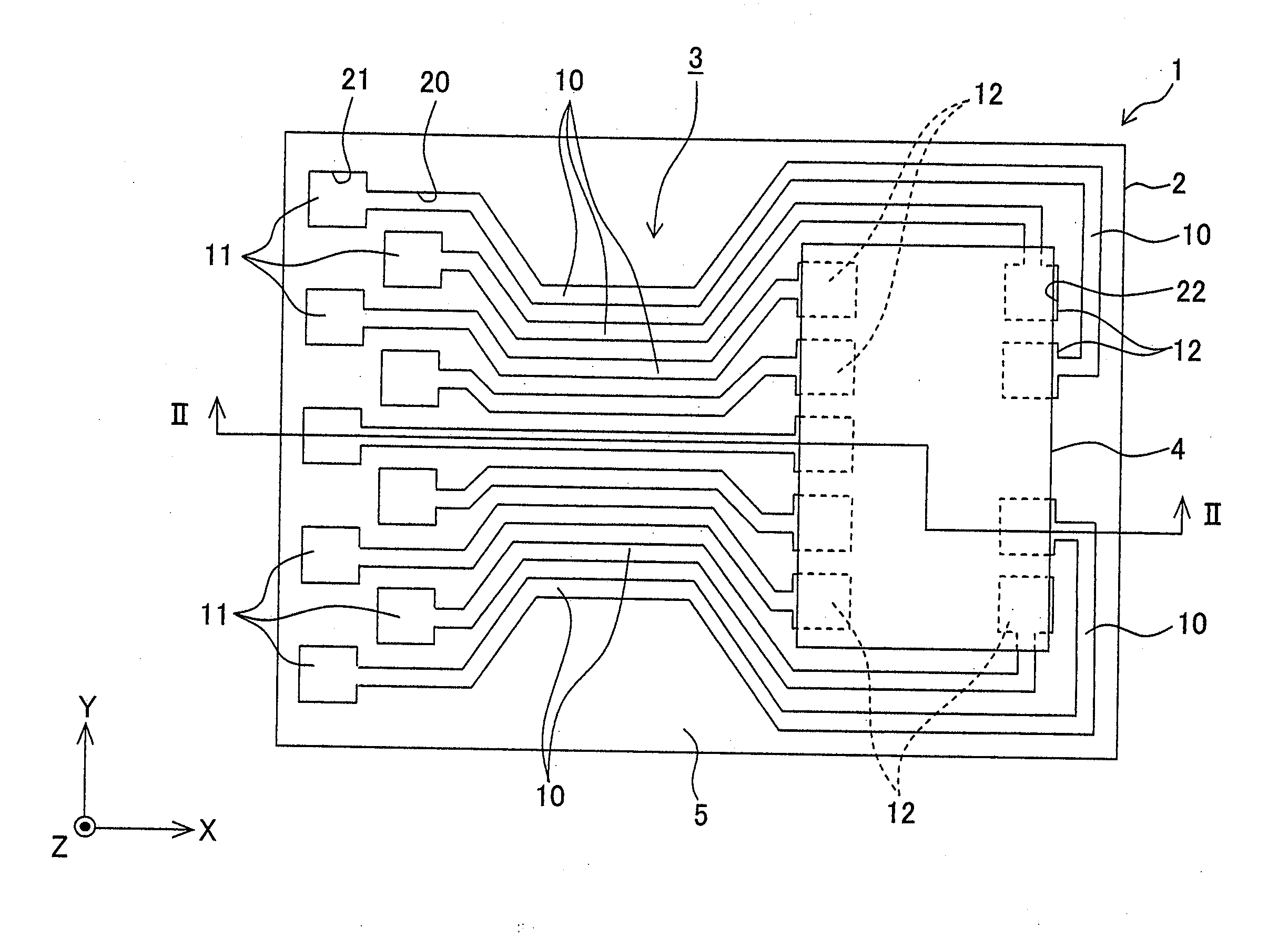
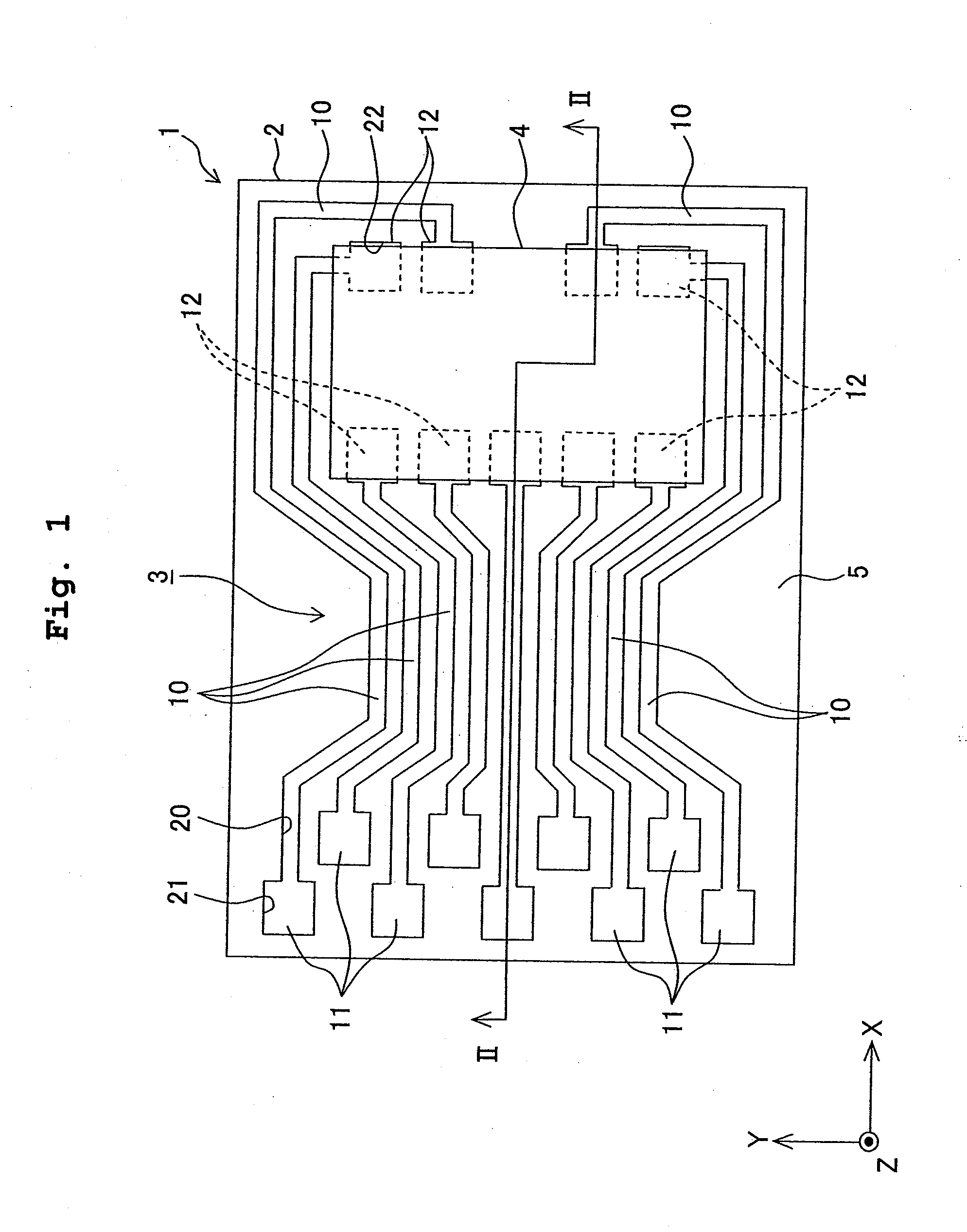
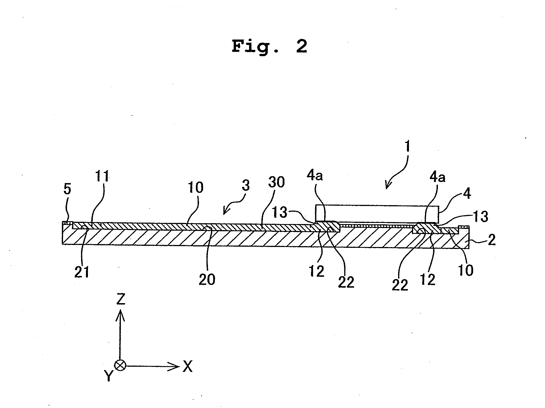
[0060]A first embodiment of the present invention will be explained. The first embodiment is an example of the application of the present invention to a case in which a conductive pattern is formed on a surface of a flat plate-shaped base material for constructing a board. The following description will be made assuming that the X axis direction shown in FIG. 1 is defined as the longitudinal direction or the left and right directions, and the direction (upward direction in FIG. 2), which is directed to the front side of the paper surface of FIG. 1 in the Z axis direction, is defined as the upward direction.

[0061]At first, the board 1 will be explained. As shown in FIGS. 1 and 2, the board 1 has the flat plate-shaped base material 2 which is composed of an insulating material, and the conductive pattern 3 which is formed on an upper surface of the base material 2. A driver IC 4 (electronic part), which serves as a driving circuit electrically connected to the conductive pattern 3, is...

first modified embodiment

[0081]As shown in FIG. 5, surface layers 41 may be formed on the bumps 13 such that the bumps 13, which are composed of, for example, silver or gold, are formed on the surface of the conductive material 30 (connecting terminals 12) charged into the recesses 22, and then conductive liquid droplets, which contain a metal material such as melted solder different from the material of the bumps 13, are landed on the surfaces of the bumps 13.

second modified embodiment

[0082]It is not necessarily indispensable that the liquid-repellent film 5 is formed on the upper surface of the base material 2. It is also allowable that the liquid-repellent film-forming step is omitted. Also in this case, on condition that the surface roughness of the inner surface of the groove 20 and the recesses 21, 22 is larger than the surface roughness of the upper surface of the base material 2, the liquid repellence of the inner surface of the groove 20 and the recesses 21, 22 is lower than the liquid repellence of the upper surface of the base material 2. For example, when the groove 20 and the recesses 21, 22 are formed by means of the laser processing, then the inner surface for defining the groove 20 and the recesses 21, 22 can be made rough, and the wettability can be enhanced. In this case, the liquid repellence of the upper surface of the base material 2 is relatively higher than the liquid repellence of the inner surface of the groove 20 and the recesses 21, 22. ...


PUM

PropertyMeasurementUnit
widthaaaaaaaaaa
widthaaaaaaaaaa
volumeaaaaaaaaaa

Abstract

A groove and a recess are formed on one surface of a base material, the recess being communicated with the groove and having a width and a length longer than a width of the groove. After that, liquid droplets are landed on the recess to charge a liquid into the groove communicated with the recess. Further, the liquid charged into the groove is solidified. Accordingly, the liquid can be charged into the groove having the narrow width, by merely landing the liquid droplets on the recess having a large areal size. Therefore, a fine pattern can be easily formed on the base material.

Description

BACKGROUND OF THE INVENTION[0001]1. Field of the Invention[0002]The present invention relates to a method for forming various patterns such as conductive patterns on a surface of a base material and a wired board having conductive patterns.[0003]2. Description of the Related Art[0004]The wired member, which includes, for example, boards or substrates on which electronic devices such as IC chips are mounted, and flexible printed circuits (FPC) which are usable to electrically connect devices, has a conductive pattern which is formed on a surface of a base material composed of, for example, a silicon material, a glass material, or a synthetic resin material. It is preferable that such a conductive pattern is formed to have a width and a pitch which are as fine as possible, for example, because it is intended to miniaturize the sizes of the board and the wired member.[0005]The lithography method has been hitherto used as a method for forming the fine conductive pattern as described abo...

Claims


Application Information

Patent Timeline
Patent Type & Authority Applications(United States)
IPC IPC(8): H05K3/10
CPCH05K3/107H05K3/125H05K3/1258H05K3/321H05K3/4007H05K3/4069Y10T29/49126H05K2201/09036H05K2201/0949H05K2203/013H01L24/81H01L2224/81192Y10T29/49155H05K2201/0367H01L2924/12042H01L2224/10175H01L2224/82101H01L24/82H01L2224/24225H01L24/24H01L2924/00
Inventor SUGAHARA, HIROTO
Owner BROTHER KOGYO KK
Learn More