Method for fabricating a semiconductor device

a semiconductor device and manufacturing method technology, applied in semiconductor/solid-state device manufacturing, basic electric elements, electric devices, etc., can solve problems such as difficulty in fabricating semiconductor devices, and achieve the effect of convenient fabricated

Active Publication Date: 2009-07-14
SAMSUNG ELECTRONICS CO LTD
View PDF7 Cites 4 Cited by
  • Summary
  • Abstract
  • Description
  • Claims
  • Application Information

AI Technical Summary

Benefits of technology

[0012]In addition, in accordance with embodiments of the invention, the width of an isolation layer may be readily controllable, so a semiconductor device comprising an isolation layer having a width of less than about 50 nm, and further comprising a first channel region comprising single-crystalline silicon and a second channel region comprising single-crystalline silicon-germanium, may be readily fabricated.

Problems solved by technology

However, using a conventional method, it is difficult to fabricate a semiconductor device that includes an isolation layer having a width of less than about 50 nm and also includes a channel region including single-crystalline silicon and another channel region including single-crystalline silicon-germanium.

Method used


Image

  • Method for fabricating a semiconductor device
  • Method for fabricating a semiconductor device
  • Method for fabricating a semiconductor device

Examples


Embodiment Construction

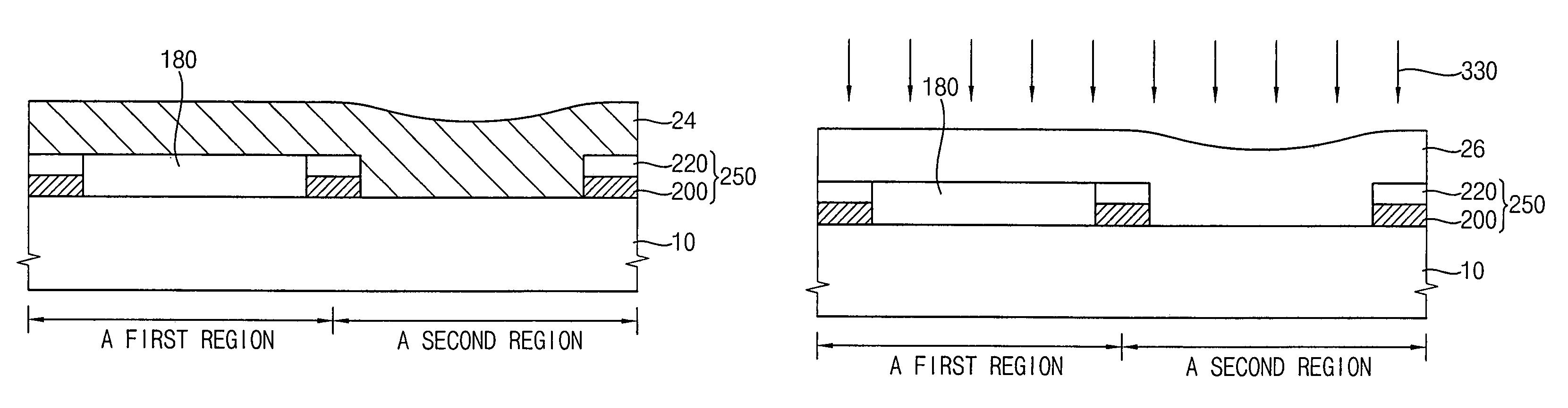
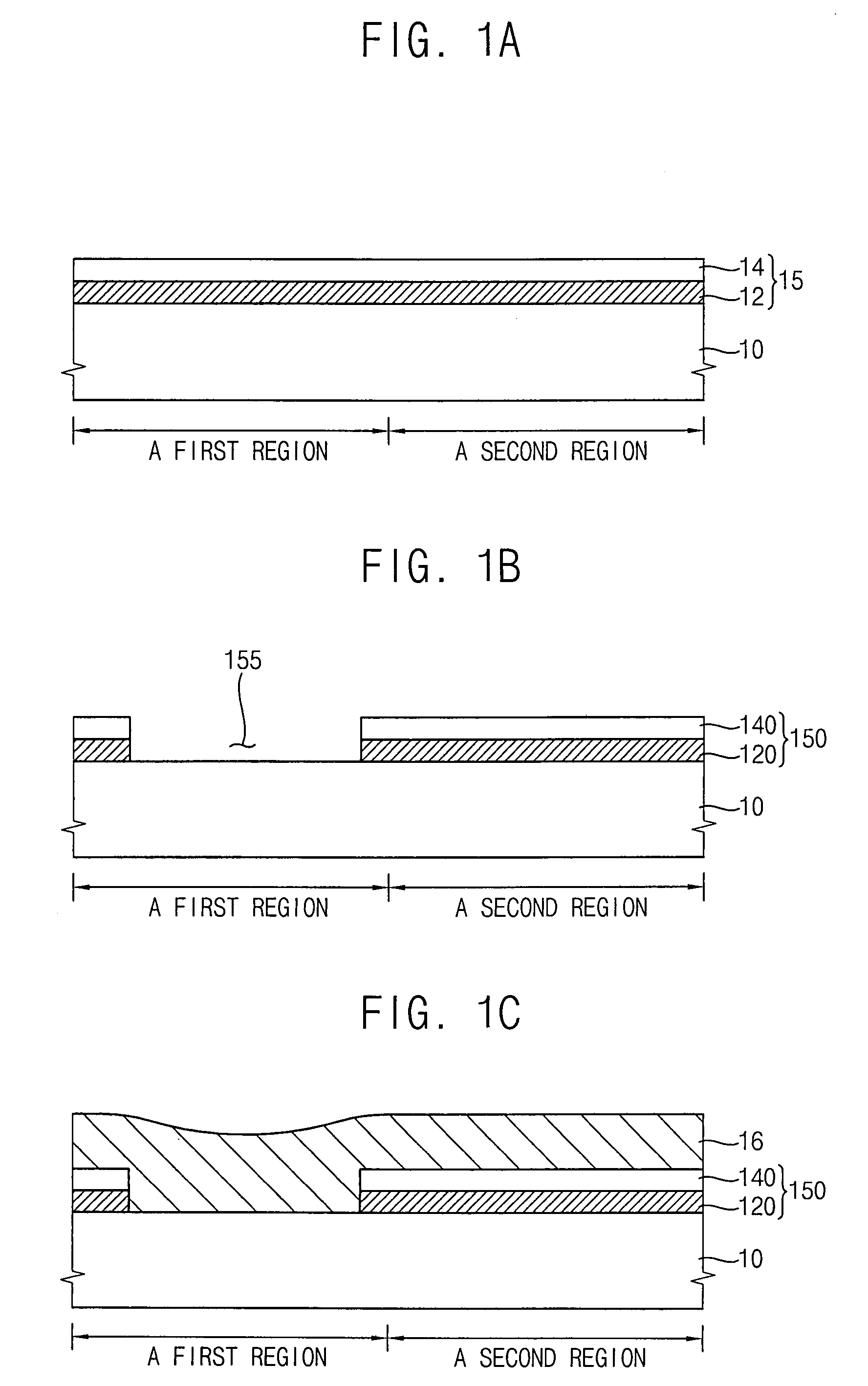
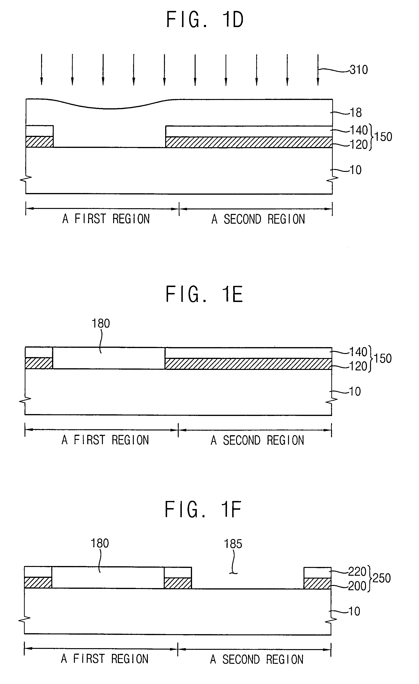
[0017]In the drawings, the sizes of layers and regions are not necessarily drawn to scale, and like reference symbols refer to like or similar elements throughout.

[0018]As used herein, when a first element or layer is referred to as being “on” or “connected to” a second element or layer, the first element or layer may be directly on or directly connected to the second element or layer or intervening elements or layers may be present. In contrast, when a first element is referred to as being “directly on,” or “directly connected to” a second element or layer, there are no intervening elements or layers present. As used herein, the term “and / or” includes any combination of one or more of the associated listed items.

[0019]In addition, although terms such as “first,” and “second,” may be used herein to describe various elements, components, regions, layers, and / or sections, those elements, components, regions, layers and / or sections should not be limited by those terms. Those terms are ...


PUM

PropertyMeasurementUnit
widthaaaaaaaaaa
temperatureaaaaaaaaaa

Abstract

A method of fabricating a semiconductor device includes forming an insulation layer structure on a single-crystalline silicon substrate, forming a first insulation layer structure pattern comprising a first opening by etching a portion of the insulation layer structure, filling the first opening with a non-single-crystalline silicon layer, and forming a single-crystalline silicon pattern by irradiating a first laser beam onto the non-single-crystalline silicon layer. The method also includes forming a second insulation layer structure pattern comprising a second opening by etching a portion of the first insulation layer structure, filling the second opening with a non-single-crystalline silicon-germanium layer, and forming a single-crystalline silicon-germanium pattern by irradiating a second laser beam onto the non-single-crystalline silicon-germanium layer.

Description

BACKGROUND OF THE INVENTION[0001]1. Field of the Invention[0002]Embodiments of the invention relate to methods for fabricating a semiconductor device. In particular, embodiments of the invention relate to methods for fabricating a semiconductor device comprising at least one of a complementary metal oxide semiconductor (CMOS) transistor and a silicon-on-insulator substrate.[0003]This application claims priority to Korean Patent Application No. 2006-0030095, filed on Apr. 3, 2006, the subject matter of which is hereby incorporated by reference in its entirety.[0004]2. Description of the Related Art[0005]In general, a CMOS transistor has a structure comprising an N-channel metal oxide semiconductor (NMOS) transistor and a P-channel metal oxide semiconductor (PMOS) transistor. When a channel region of the NMOS transistor includes single-crystalline silicon, the NMOS transistor will have relatively good electrical performance. In addition, when a channel region of the PMOS transistor in...

Claims


Application Information

Patent Timeline
Patent Type & Authority Patents(United States)
IPC IPC(8): H01L21/84
CPCH01L21/823807H01L21/84H01L21/823878H01L21/18
Inventor KANG, SUNG-KWANSHIN, YU-GYUNLEE, JONG-WOOKSON, YONG-HOON
Owner SAMSUNG ELECTRONICS CO LTD
Why Eureka
Try Eureka