Latency control circuit and semiconductor memory device including the same

a technology of latency control circuit and semiconductor memory device, which is applied in the direction of digital storage, pulse automatic control, instruments, etc., can solve the problem of increasing power consumption

Active Publication Date: 2011-08-04
SK HYNIX INC
View PDF2 Cites 31 Cited by
  • Summary
  • Abstract
  • Description
  • Claims
  • Application Information

AI Technical Summary

Benefits of technology

[0005]An embodiment of the present invention is directed to a latency control circuit capable to perform an accurate control operation and a semiconductor device including the same.

Problems solved by technology

For performing reliable operations, the conventional method should continuously provide the clocks even for an asynchronous mode and, therefore, the power consumption increases.

Method used


Image

  • Latency control circuit and semiconductor memory device including the same
  • Latency control circuit and semiconductor memory device including the same
  • Latency control circuit and semiconductor memory device including the same

Examples


Embodiment Construction

[0017]Exemplary embodiments of the present invention will be described below in more detail with reference to the accompanying drawings. The present invention may, however, be embodied in different forms and should not be constructed as limited to the embodiments set forth herein. Rather, these embodiments are provided so that this disclosure will be thorough and complete, and will fully enable those having ordinary skill in the art to practice the invention without undue experimentation. Throughout the disclosure, like reference numerals refer to like parts throughout the various figures and embodiments of the present invention.

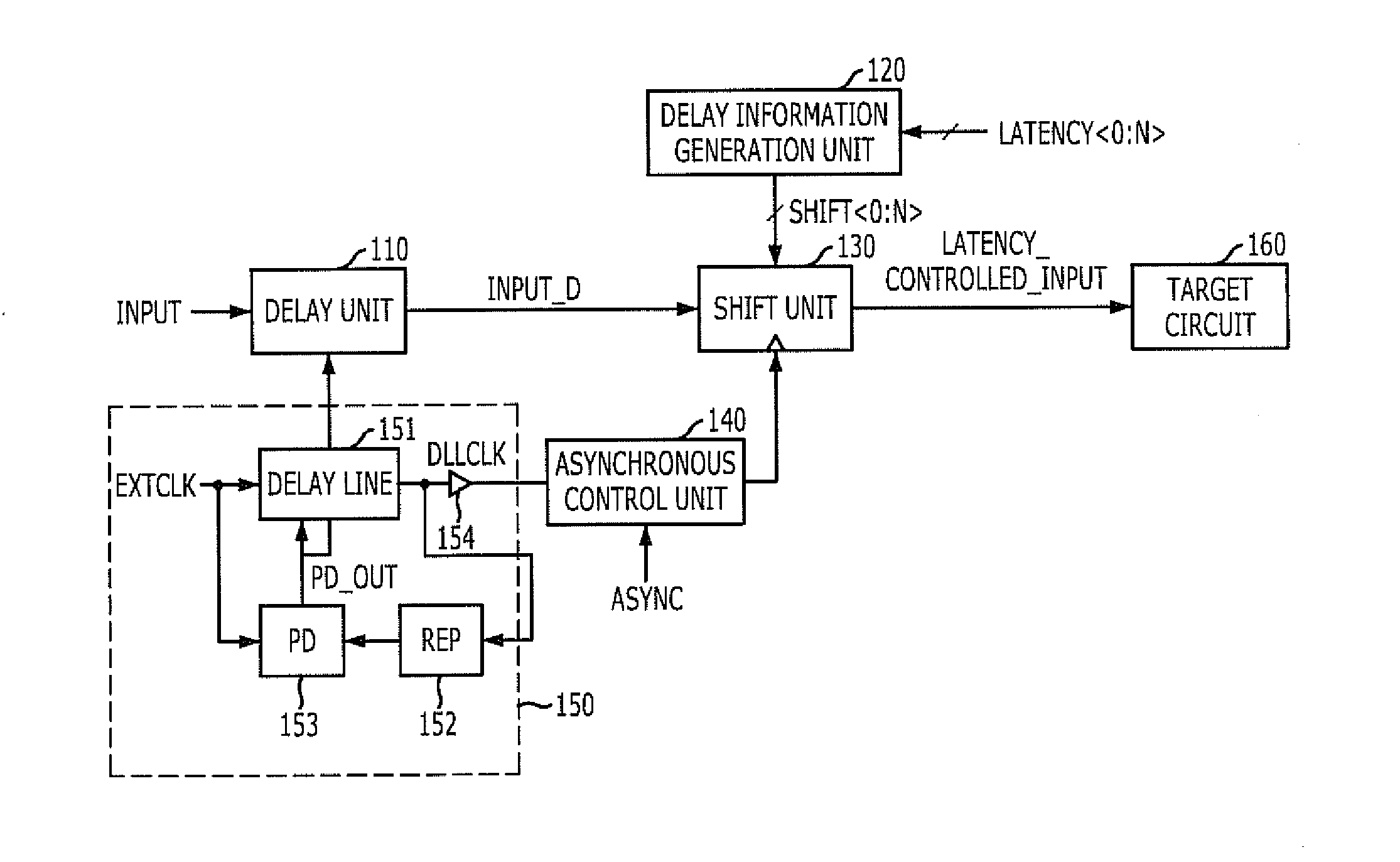
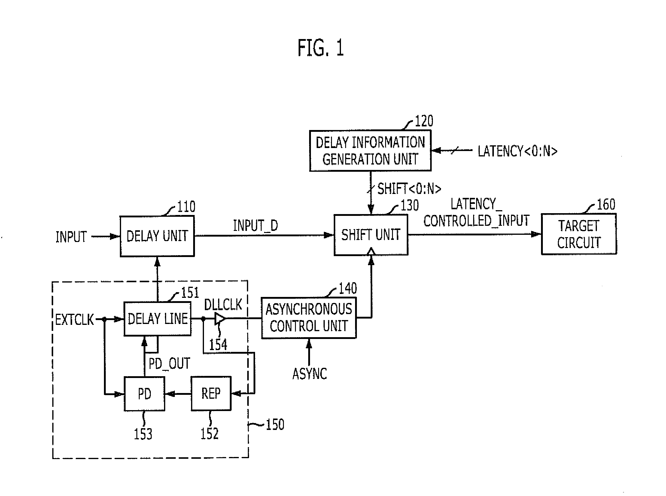
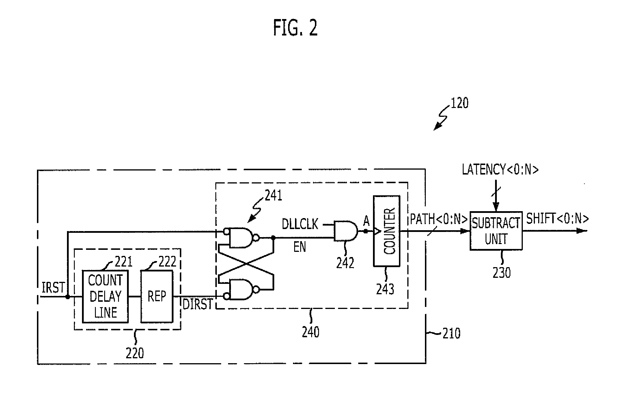
[0018]FIG. 1 is a block diagram illustrating a latency control circuit for use in a semiconductor device in accordance with an embodiment of the present invention.

[0019]The latency control circuit includes a delay unit 110, a delay information generation unit 120, a shift unit 130, an asynchronous control unit 140, and a delay locked loop (DLL) 150.

[0020]The...


PUM


Abstract

A latency control circuit includes a delay unit configured to delay an input signal for a delay corresponding to a phase difference between an external clock and an internal clock and generate a delayed input signal, a delay information generation unit configured to generate a delay information based on a latency information and a delay amount of the input signal caused by a chip including the latency control circuit, a shift unit configured to shift the delayed input signal for a time period corresponding to the delay information in synchronism with the internal clock and an asynchronous control unit configured to selectively control the shift unit to output the delayed input signal without performing a shift operation.

Description

CROSS-REFERENCE TO RELATED APPLICATION[0001]The present application claims priority of Korean Patent Application No. 10-2010-0010405, filed on Feb. 4, 2010, which is incorporated herein by reference in its entirety.BACKGROUND OF THE INVENTION[0002]Exemplary embodiments of the present invention relate to a method for fabricating a latency control circuit, and more particularly, to a latency control circuit efficiently performing a latency control operation.[0003]When operations are performed between plural semiconductor devices, a predetermined latency occurs from receiving an operational request signal to starting an operation corresponding to the operational request signal. For example, a memory controller outputs a termination command signal and a memory device starts terminating a data pad after a column address strobe (CAS) latency from an input timing of the termination command signal. In order to ensure the reliable processing of the operations between the semiconductor device...

Claims


Application Information

Patent Timeline
Patent Type & Authority Applications(United States)
IPC IPC(8): H03L7/06
CPCH03L7/06G11C7/222G11C11/4076H03L7/0814G11C7/22G11C2207/2272H03L7/0816
Inventor KIM, KYUNG-HOONKIM, KYUNG-WHAN
Owner SK HYNIX INC
Why Eureka
Try Eureka