

Substrate for electro-optical devices, electro-optical device and electronic apparatus
- Summary
- Abstract
- Description
- Claims
- Application Information
AI Technical Summary
Benefits of technology
Problems solved by technology
Method used
Image

Examples
first embodiment
[0048]First, an entire configuration of an electrophoretic display panel of the present embodiment will be described with reference to FIGS. 1 and 2.
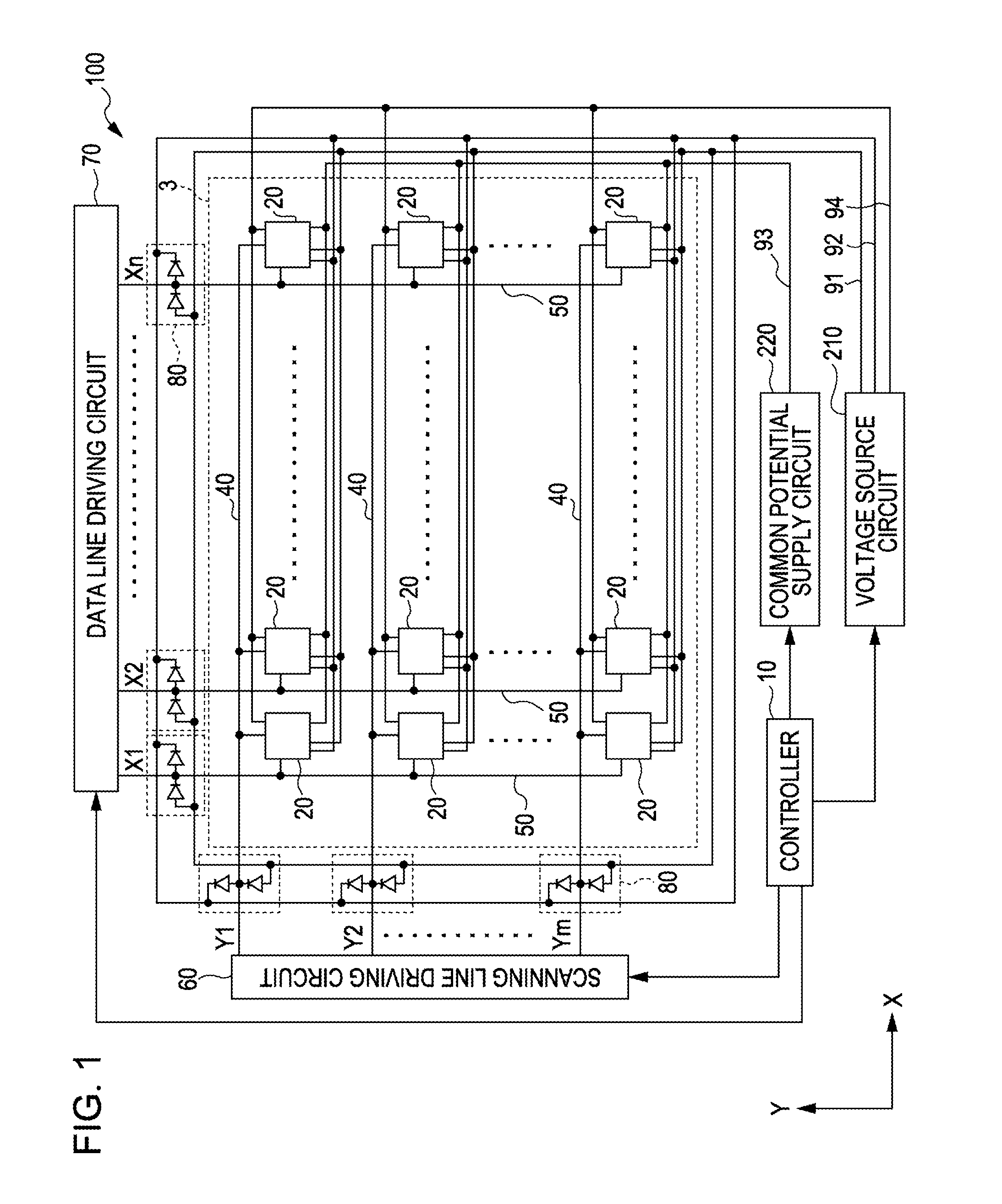
[0049]FIG. 1 is a block diagram illustrating the entire configuration of an electrophoretic display panel of a first embodiment.
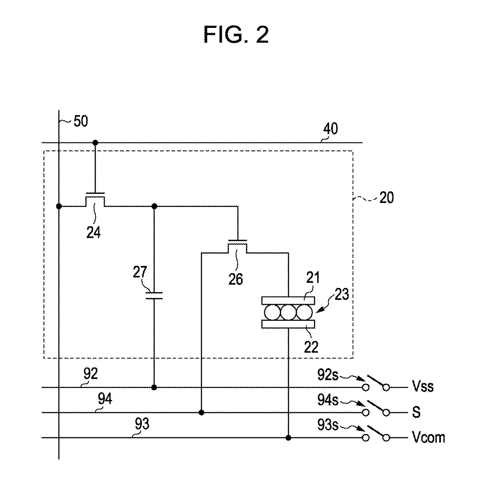
[0050]In FIG. 1, an electrophoretic display panel 100 of the embodiment is provided with a display unit 3, a controller 10, a scanning line driving circuit 60, a data line driving circuit 70, a voltage source circuit 210, and a common potential supply circuit 220. Here, the display unit 3 is an example of the “display region” of the invention.
[0051]In the display unit 3, m rows and n columns of pixels 20 are arranged in a matrix (two dimensional planar) shape. Also, in the display unit 3, m scanning lines 40 (that is, scanning lines Y1, Y2, . . . , Ym) and n data lines 50 (that is, data lines X1, X2, . . . , Xn) are provided to intersect with each other. Specifically, the m scanning lines 40 extend in a row dir...
second embodiment
[0099]Next, an electrophoretic display panel according to a second embodiment will be described with reference to FIG. 9.
[0100]FIG. 9 is an enlarged cross-sectional diagram of a TFT substrate of the electrophoretic display panel of the embodiment. In the first embodiment described above, the case where the static electricity protection circuit 80 with a bottom gate type transistor which is diode-connected is provided in the peripheral region is exemplified. However, in the present embodiment, the case where the static electricity protection circuit 80 with a top gate type transistor which is diode-connected is provided in the peripheral region is exemplified. Here, since the electrophoretic display panel of the embodiment has the same basic configuration as the electrophoretic display panel of the first embodiment, the same members have the same reference numerals attached and a detailed description is not repeated.
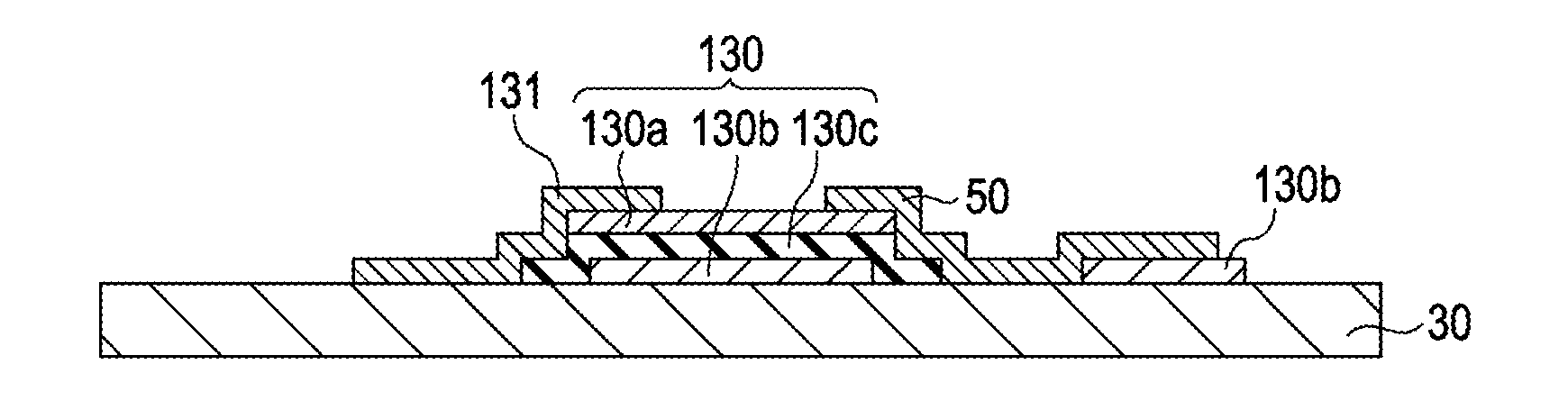
[0101]The first connection line 131 and the data line 50 are formed ...
third embodiment
[0106]Next, an electrophoretic display panel according to a third embodiment will be described with reference to FIGS. 11 and 12. In the first and second embodiments described above, the case where the static electricity protection circuit 80 with a transistor which is diode-connected is provided in the peripheral region is exemplified. However, the present embodiment is different in that an inverter circuit is provided in the peripheral region. Here, since the electrophoretic display panel of the embodiment has the same basic configuration as the electrophoretic display panel of the embodiments described above, the same members have the same reference numerals attached and a detailed description is not repeated.
[0107]First, with reference to FIG. 11, the electrical configuration of an inverter circuit 210 provided in the peripheral region of the electrophoretic display panel of the embodiment will be described. FIG. 11 is a circuit diagram illustrating the electrical configuration ...
PUM
 Abstract
Description
Claims
Application Information