Semiconductor apparatus having semiconductor module cooled by heat sinks which have increased strength together with increased thermal mass

Inactive Publication Date: 2011-08-11
DENSO CORP
View PDF6 Cites 15 Cited by
  • Summary
  • Abstract
  • Description
  • Claims
  • Application Information

AI Technical Summary

Benefits of technology

[0015]In this case, the increased thickness of a secondary fin can enable a sufficient number of screw threads to be formed in the threaded hole for securely tightening a screw or bolt. It thereby becomes possible to securely fix the semiconductor apparatus within a case at a predetermined position and orientation by utilizing only a screw or bolt, i.e., without requiring the use of other components such as nuts.
[0016]From another aspect, a plurality of semiconductor apparatuses in accordance with the present invention can be utilized to produce a three-phase rectifier apparatus, having three circuit sections corresponding to respective ones of three phases. Each of the circuit sections is formed of interconnected circuit elements constituting an upper arm and interconnected circuit elements constituting a lower arm. The upper arm and each lower arm may be implemented by respective semiconductor modules of a pair of semiconductor apparatuses according to the present invention, i.e. with the three-phase rectifier apparatus being implemented by a total of s

Problems solved by technology

However although the noise blocking plate serves to efficiently transfer heat from the semiconductor module to the heat sink, while also serving as a contact pressure determining member, so that the overall size of the semiconductor apparatus can be made compact and the manufacturing cost can be low, such a configuration does not provide satisfactory performance with respect to efficient dissipation of heat from the semiconductor module.
However as the fins are made thinner, these will more readily become distorted due t

Method used


Image

  • Semiconductor apparatus having semiconductor module cooled by heat sinks which have increased strength together with increased thermal mass
  • Semiconductor apparatus having semiconductor module cooled by heat sinks which have increased strength together with increased thermal mass
  • Semiconductor apparatus having semiconductor module cooled by heat sinks which have increased strength together with increased thermal mass

Examples


first embodiment

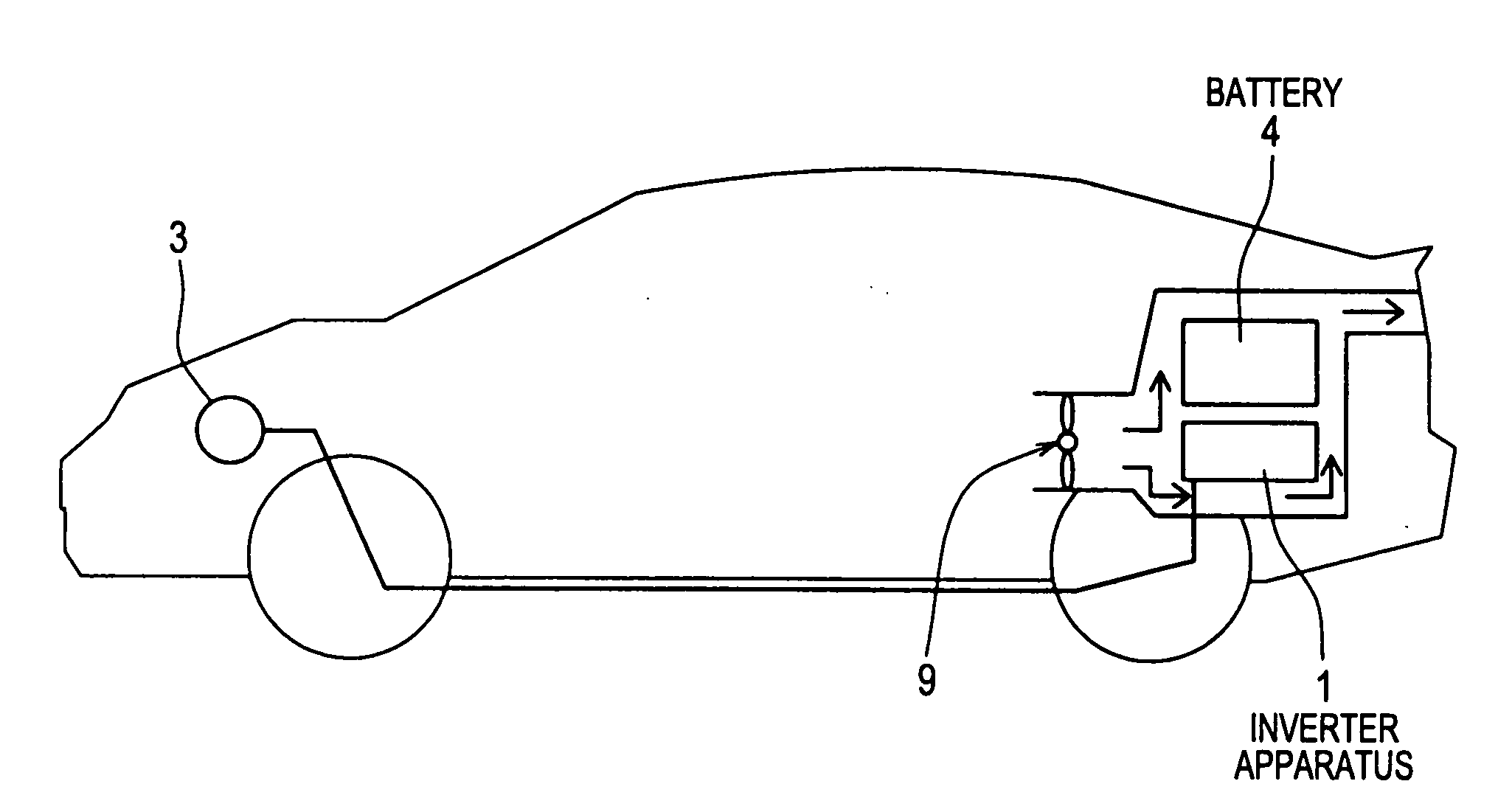
[0029]A first embodiment of a semiconductor apparatus will be described, which is suitable for use in an inverter apparatus for driving a high-power electric motor. The inverter apparatus serves to convert DC electrical power to AC power, and is typically a three-phase (U, V, W phases) inverter apparatus. The motor may be a drive motor of an electric vehicle that is powered by fuel cells such as is illustrated in the example of FIG. 1, or of a hybrid (gas / electric) vehicle.

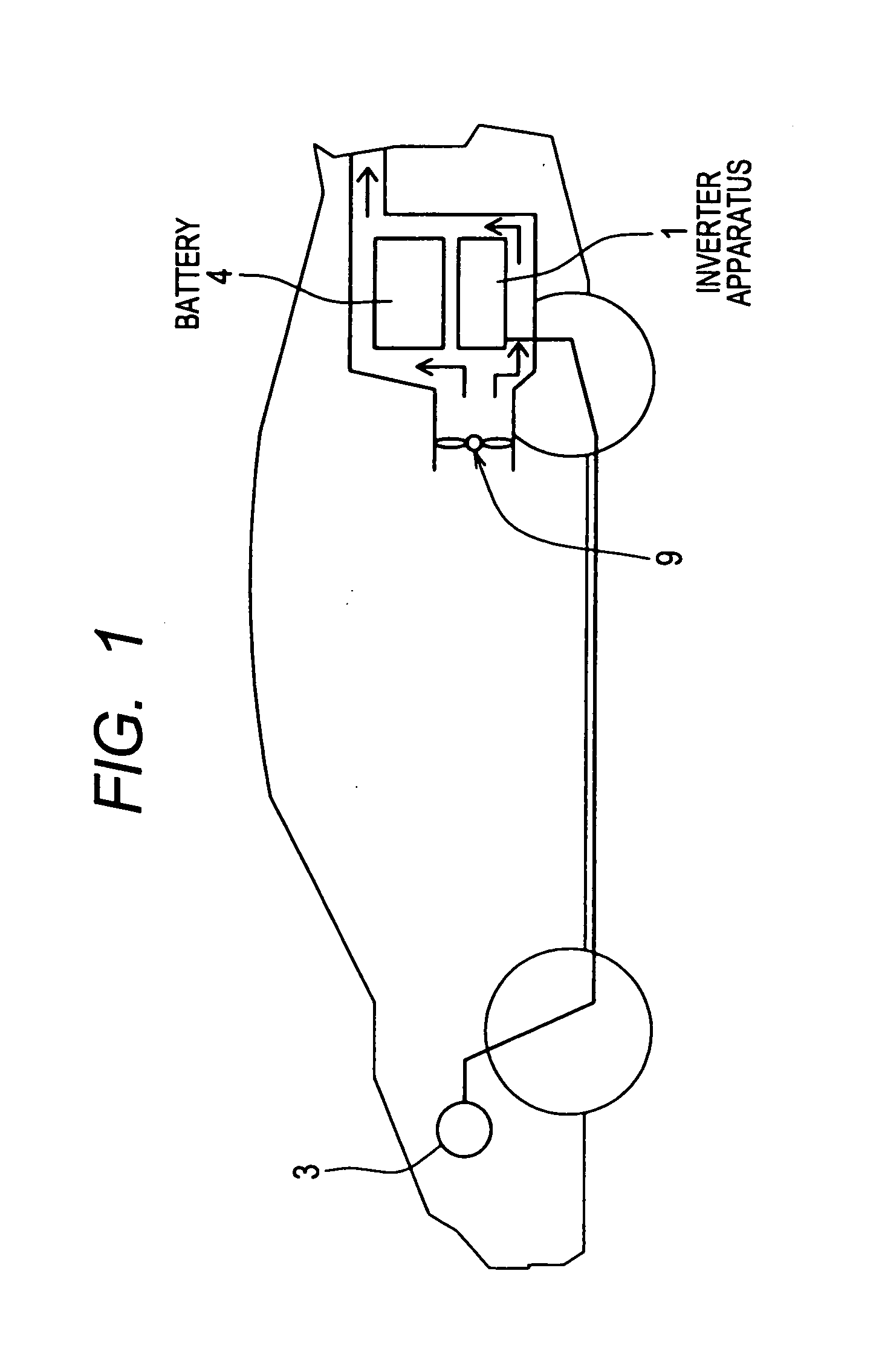
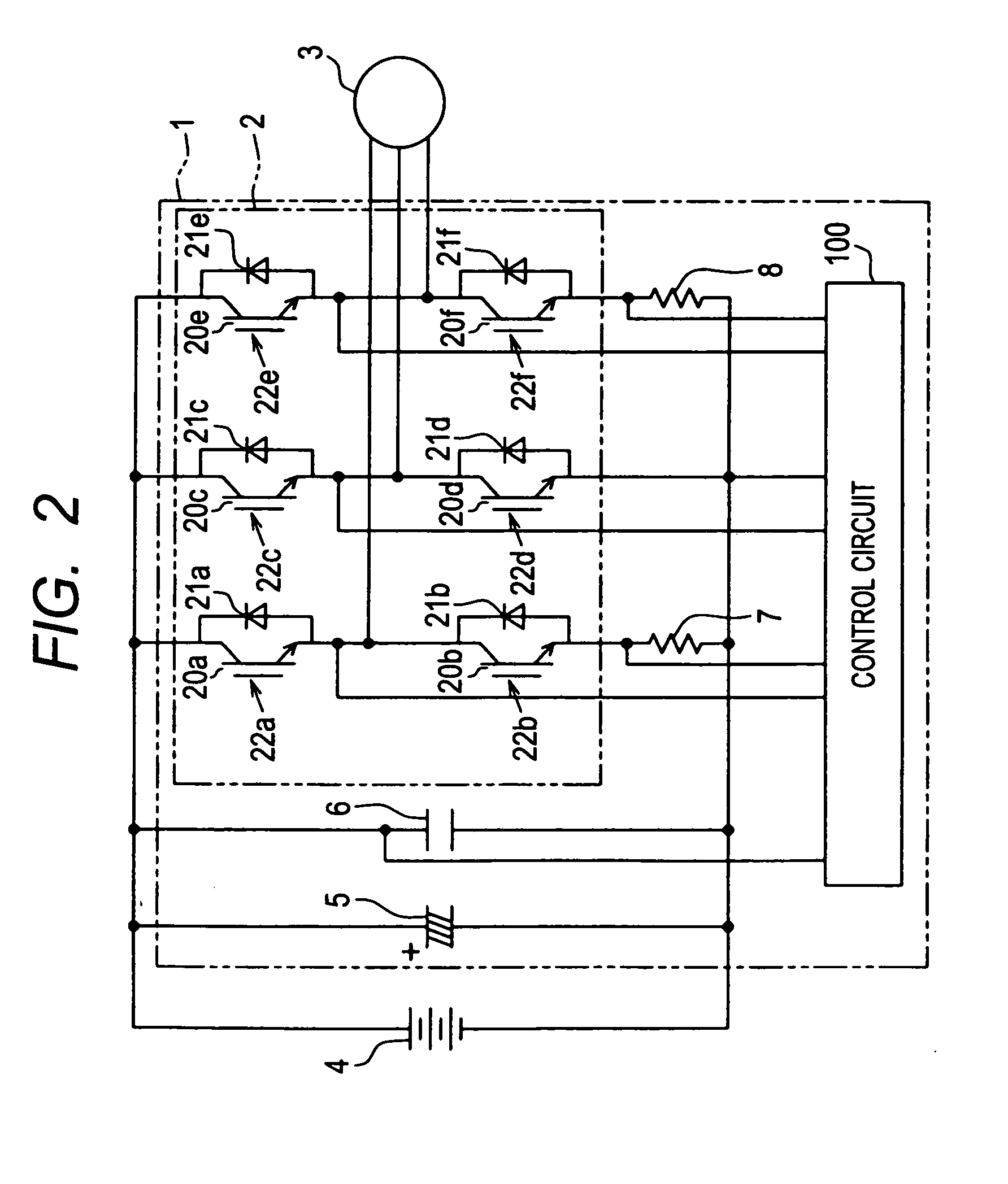
[0030]In the conceptual diagram of FIG. 1, an inverter apparatus 1 which is installed in a vehicle incorporates a three-phase inverter circuit, which drives a motor 3 to provide motive power for the vehicle. FIG. 2 is a circuit diagram of the three-phase inverter circuit, which incorporates six semiconductor apparatuses each in accordance with a first embodiment of the invention, as described hereinafter.

[0031]As shown in FIG. 1, the inverter apparatus 1 is installed at the rear end of the vehicle, adjacent to a b...

second embodiment

[0076]A second embodiment of a semiconductor apparatus will be described referring to FIG. 8, which shows an inverter circuit unit 30A having identical functions and operation to those of the inverter circuit unit 30 described above. In FIG. 8, each of respective semiconductor apparatuses 10A differs from the semiconductor apparatus 10 of the first embodiment only in that an aperture (with this embodiment, a through-hole 114) extending in the thickness direction Y is formed in one of the secondary fins 113 of one of the heat sinks 11 of the semiconductor apparatus 10A. Specifically, for each semiconductor apparatus 10A, the through-hole 114 is formed in one of the secondary fins 113 (i.e., in one of the pair of fins which contact the lower inner face of the case 31A). The lower inner face case 31A of the case 31 of the 30ax is formed with an array of protrusions 38 (each extending in the thickness direction Y). The respective positions of the protrusions 38, and the dimensions of ea...

third embodiment

[0078]A third embodiment of a semiconductor apparatus will be described referring to FIG. 9, which shows an inverter circuit unit 30B having identical functions and operation to those of the inverter circuit unit 30 described above. In FIG. 9, each of respective semiconductor apparatuses 10B differs from the semiconductor apparatus 10 of the first embodiment only in that a threaded hole 115 (extending in the thickness direction Y) is formed in one of the secondary fins 113 of one of the heat sinks 11 of the semiconductor apparatus 10B, with the holes being threaded in correspondence with a set of screws 60. Specifically, for each semiconductor apparatus 10B, the threaded hole 115 is formed in one of the pair of secondary fins 113 of that semiconductor apparatus 10B which each become placed in contact with the lid 37B when the inverter circuit unit 30A is assembled. Six through-holes (each extending in the thickness direction Y) are provided in the lid 37B. The respective positions o...


PUM


Abstract

In a semiconductor apparatus, a semiconductor module containing semiconductor elements is enclosed between a pair of heat sinks which are held attached together by spring clips. Each heat sink has one side thermally coupled to a corresponding main face of the semiconductor module and has an array of primary fins and a pair of secondary fin protruding from the other side, with the secondary fins being located at opposing ends of the array of primary fins, beyond the outermost primary fins. At least part of each secondary fin is made thicker than each primary fin, to provide greater strength and greater thermal mass for each secondary fin than each primary fin.

Description

CROSS-REFERENCE TO RELATED APPLICATIONS[0001]This application is based on and incorporates herein by reference Japanese Patent Application No. 2010-28326 filed on Feb. 11, 2010.BACKGROUND OF THE INVENTION[0002]1. Field of Application[0003]The present invention relates to a semiconductor apparatus consisting of a semiconductor module combined with heat sinks which dissipate heat that is generated by the semiconductor module.[0004]2. Description of Related Art[0005]Types of semiconductor apparatus are known which incorporate a semiconductor module and a heat sink which is thermally coupled to the semiconductor module, for cooling the module. The heat sink may contact the semiconductor module through the intermediary of a sheet of thermally conductive material, and / or a layer of thermally conductive grease, etc. Such a type of semiconductor apparatus is described for example in Japanese patent publication No. 2003-347783. With the semiconductor apparatus described in that patent disclo...

Claims


Application Information

Patent Timeline
IPC IPC(8): H05K7/20
CPCH01L23/467H01L25/072H01L25/18H02M7/003H01L2924/0002H01L2924/00
Inventor MOMOSE, TAIJIROU
Owner DENSO CORP
Why Eureka
Try Eureka