
Scribe-line draining during wet-bench etch and clean processes
- Summary
- Abstract
- Description
- Claims
- Application Information
AI Technical Summary
Benefits of technology
Problems solved by technology
Method used
Image

Examples
Embodiment Construction
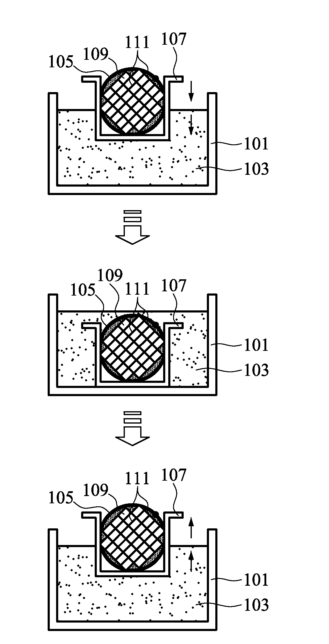
[0019]Provided are methods and systems that may be used in conjunction with the type of chemical or wet baths used in the manufacture of semiconductor devices. The methods and systems are applicable to various chemistries and although the following description will often be with respect to a wet etch; such is intended to be exemplary only and not limiting of the applications of the invention. According to other embodiments, the methods of the present invention are also applicable to other wet chemical processes such as cleaning or rinsing processes.
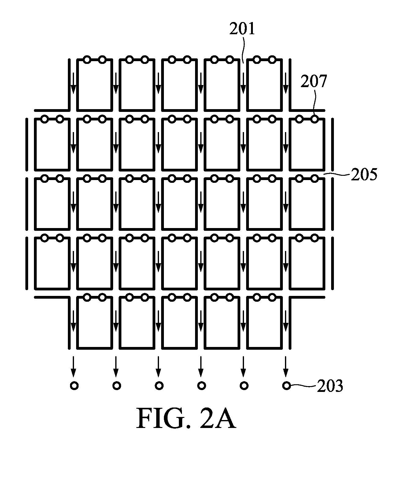
[0020]On a wafer, scribe lines demarcate the boundary between different dies and are used ultimately to separate the various dies on the same wafer into different semiconductor products by cutting or sawing according to the scribe lines. Most dies are rectangular so that the scribe lines intersect each other at 90 degrees; however, scribe lines need not be perpendicular as long as the dies fill the surface of the wafer in a repeating patt...
PUM
 Abstract
Description
Claims
Application Information