Contact Formation Method, Semiconductor Device Manufacturing Method, and Semiconductor Device

a technology of contact formation and manufacturing method, which is applied in the direction of semiconductor devices, basic electric elements, electrical apparatus, etc., can solve the problems of preventing oxygen, impedes performance improvement, and does not sufficiently clarify, so as to prevent oxygen and reduce the resistance of contact silicide or gate metal. , the effect of low contact resistan

Active Publication Date: 2011-08-18
TOHOKU UNIV +1
View PDF14 Cites 7 Cited by
  • Summary
  • Abstract
  • Description
  • Claims
  • Application Information

AI Technical Summary

Benefits of technology

[0011]According to the present invention, it is possible to form a practical contact having a low contact resistivity. Further, according to the present invention, it is possible to prevent oxygen from being mixed during silicidation.

Problems solved by technology

However, in the semiconductor device, a series resistance between two main electrodes, through which an electric current mainly flows, impedes the performance improvement.
However, Patent Document 1 does not sufficiently clarify which of the above-mentioned materials is practically preferable.
This results in a problem that an increase of a resistance of the contact silicide or the gate metal is inevitable.

Method used


Image

  • Contact Formation Method, Semiconductor Device Manufacturing Method, and Semiconductor Device
  • Contact Formation Method, Semiconductor Device Manufacturing Method, and Semiconductor Device
  • Contact Formation Method, Semiconductor Device Manufacturing Method, and Semiconductor Device

Examples


first embodiment

[0057]As shown in FIG. 7 (A), the n-channel field-effect transistor according to the present invention is formed in a device region of a silicon substrate 20 which is isolated by a device isolation region 22. As the silicon substrate 20, for example, a p-type silicon substrate is used. In the example illustrated in the figure, a p+ well region 24 is formed in the device region. Within the p+ well region 24, a gate insulating film 26 formed of a silicon oxide film or the like and a gate electrode 28 formed of polysilicon or the like are provided. Although not shown in the figure, a shallow implant region is formed in a region to be a source / drain.

[0058]Thereafter, in order to ensure insulation with respect to the gate electrode 26, a side wall 30 comprising a silicon oxide film or a silicon nitride film is formed on the gate insulating film26 and the gate electrode 28. Subsequently, over the entire surface, an interlayer insulating film 31 of BPSG (Boro-Phospho Silicate Glass) is for...

second embodiment

[0072]Referring to FIG. 8, a semiconductor device according to the present invention will be described. The semiconductor device illustrated in FIG. 8 is a so-called bulk-current controlled type accumulation mode n-channel transistor.

[0073]In the bulk-current controlled type accumulation mode n-channel transistor illustrated in the figure, on a supporting substrate 50 formed of p-type silicon, an n-type semiconductor layer 54 is formed and isolated by a buried oxide film 52 having a thickness of about 100 nm. Herein, the semiconductor layer 54 forms a channel region. A surface of the channel region illustrated in the figure has a (100) orientation. The semiconductor layer 54 has a film thickness of 50 nm. On both sides of the channel region formed of the n-type semiconductor layer 54, source / drain regions 56 are formed each of which has a conductivity type identical with that of the channel region and each of which is formed of an n+ semiconductor having an impurity atomic concentra...

third embodiment

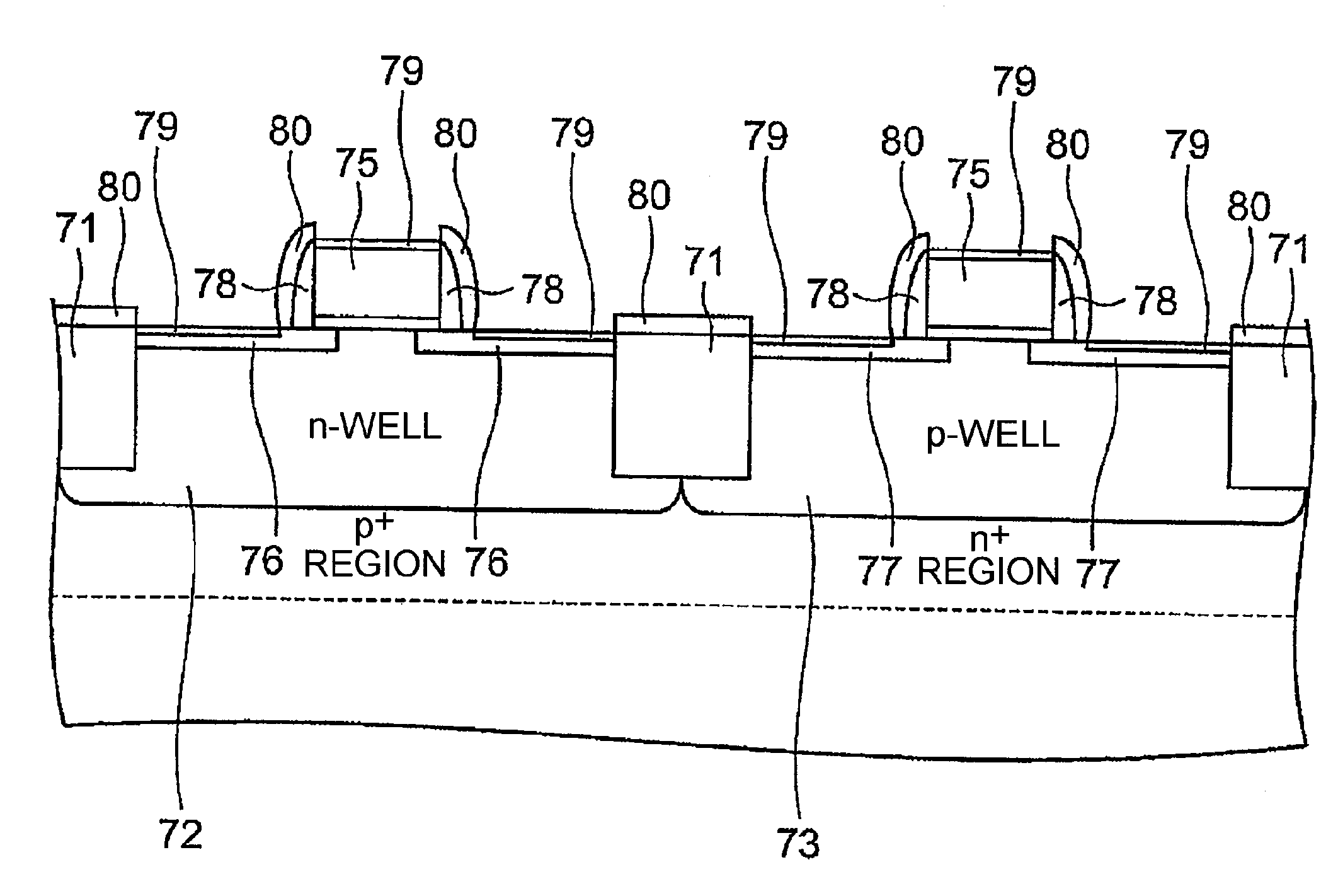
[0081]Referring to FIG. 9, a semiconductor device according to the present invention will be described. The semiconductor device illustrated in the figure is a CMOS using device isolation by shallow trench isolation (STI), two-layer wiring, and chemical mechanical polishing (CMP).

[0082]A manufacturing process for obtaining the structure shown in FIG. 9 will be described using FIGS. 10 and 11. First, referring to FIG. 10, a device isolation region 71 of a STI structure is formed. After an n-well 72 and a p-well 73 are formed, activation is performed. Subsequently, as a gate insulating film 74, a silicon oxide film is formed to a thickness of 2 nm. On the gate insulating film 74, a gate electrode 75 is formed by using polysilicon.

[0083]Next, for the purpose of forming p+ regions 76 and n+ regions 77 in the n-well 72 and the p-well 73, boron and phosphorus are ion-implanted into the n-well 72 and the p-well 73 by 6×1015 cm2, respectively. As a consequence, the high-concentration region...


PUM

PropertyMeasurementUnit
work functionaaaaaaaaaa
areaaaaaaaaaaa
work functionaaaaaaaaaa

Abstract

A semiconductor device manufacturing method which achieves a contact of a low resistivity is provided.
In a state where a first metal layer in contact with a semiconductor is covered with a second metal layer for preventing oxidation, only the first metal layer is silicided to form a silicide layer with no oxygen mixed therein. As a material of the first metal layer, a metal having a work function difference of a predetermined value from the semiconductor is used. As a material of the second metal layer, a metal which does not react with the first metal layer at an annealing temperature is used.

Description

TECHNICAL FIELD[0001]This invention relates to an MIS semiconductor device widely used in an IC, an LSI, and the like and, in particular, to a structure of a source / drain electrode and / or a structure of a gate electrode.BACKGROUND ART[0002]In a semiconductor device, performance improvement, such as improvement in operating frequency, has been strongly desired. However, in the semiconductor device, a series resistance between two main electrodes, through which an electric current mainly flows, impedes the performance improvement. Patent Document 1 describes the necessity of reducing the series resistance and, specifically, the necessity of substantially reducing a contact resistance between a semiconductor region and an electrode.[0003]Patent Document 1 proposes to use, as a material of an electrode contacting an n+ silicon region, Er, Mg, Mn, Cd, Hf, Y, or Zr each having a work function close to −4.05 eV which is a work function of the n+ silicon region, and to use, as a material of...

Claims


Application Information

Patent Timeline
Patent Type & Authority Applications(United States)
IPC IPC(8): H01L27/092H01L21/28H01L23/52H01L29/78
CPCH01L21/28079H01L21/28518H01L21/823814H01L21/823835H01L27/092H01L29/41733H01L2924/0002H01L29/4958H01L29/66772H01L29/7833H01L29/458H01L2924/00
Inventor OHMI, TADAHIROTERAMOTO, AKINOBUISOGAI, TATSUNORITANAKA, HIROAKI
Owner TOHOKU UNIV
Why Eureka
Try Eureka