Nitride semiconductor based light-emitting device and manufacturing method thereof

Active Publication Date: 2007-09-27
USHIO OPTO SEMICON
View PDF6 Cites 6 Cited by
  • Summary
  • Abstract
  • Description
  • Claims
  • Application Information

AI Technical Summary

Benefits of technology

[0047]The above-described procedures are included in a manufacturing method of the nitride semiconductor based light-emitting device such as a light-emitting diode (abbreviated as “an LED”) or a laser diode (abbreviated as “an LD”), thereby increasing the carrier concentration of the P-type nitride semiconductor in the device, resulting in a reduced contact resistivity of a P-type ohmic electrode.
[0048]In the manufacturing method according to the present invention, the hydrogen of the high concentration mixed in the P-type nitride semiconductor can be sufficiently eliminated, so that the concentration of the hydrogen in the P-type nitride semiconductor can be readily reduced more than in the prior art. Th

Problems solved by technology

As a result, it was revealed that a very thin residual is produced on the semiconductor, and thu

Method used


Image

  • Nitride semiconductor based light-emitting device and manufacturing method thereof
  • Nitride semiconductor based light-emitting device and manufacturing method thereof
  • Nitride semiconductor based light-emitting device and manufacturing method thereof

Examples


first embodiment

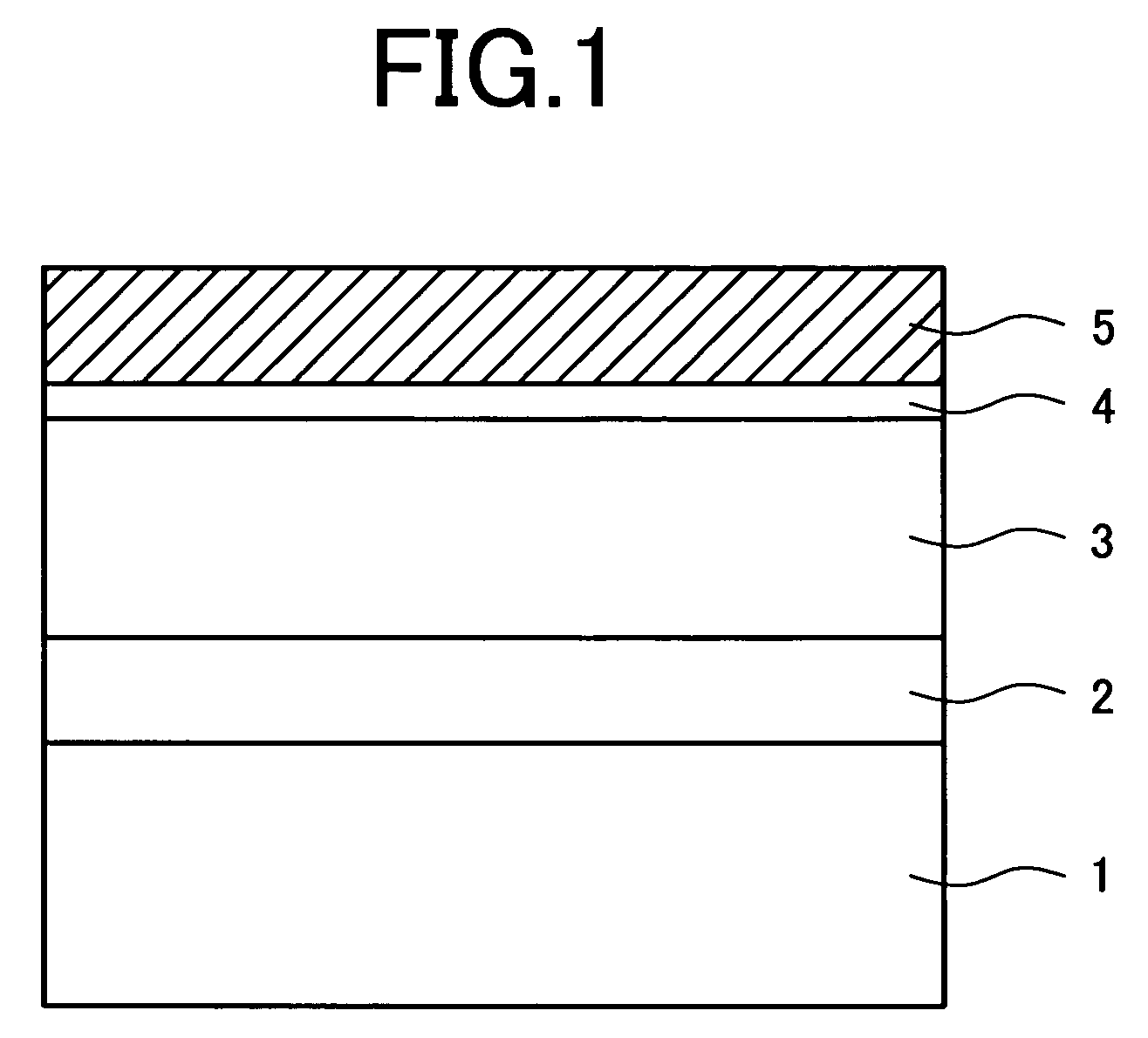
[0060]FIG. 1 is a view schematically showing a most distinctive structure fabricated in processes of a manufacturing method according to the present invention, the processes being encompassed in the manufacturing method of a nitride semiconductor based light-emitting device. Specifically, FIG. 1 is a cross-sectional view showing a stack structure after a process (B), described below.

[0061]In the present preferred embodiment, for the sake of easy comparison between an effect produced by the manufacturing method according to the present invention and an effect produced by the prior art, explanation will be made by using the same substrate as that for use in explicitly describing the problems experienced by the prior art under the section of “Background of the Invention”, that is, by using a sapphire substrate having only an Mg doped GaN layer [having an Mg doping concentration (i.e., an SIMS value) of 7.4×1019 cm−3 and a film thickness of 2.0 μm] growing thereon via an AlN buffer laye...

second embodiment

[0081]Subsequently, a description will be given of a manufacturing method of a first metal film formed by stacking two kinds of metals out of the above-described four kinds of metals in one preferred embodiment and its effect.

[0082]Also in the present preferred embodiment is used the same substrate as that in the first embodiment.

[0083]A first metal film 4 of a dual layer structure consisting of a Pd film 9 having a film thickness of 10 nm as a first layer and a Pt film 33 having a film thickness of 15 nm as a second layer is formed on an Mg doped GaN layer in contact therewith. Thereafter, a tungsten oxide film 5 having a film thickness of 500 nm less than that in the above-described preferred embodiment is formed by sputtering (as shown in FIG. 3). As a result of an annealing experiment in the same manner as the above-described preferred embodiment, it has been found that a hydrogen concentration decreases down to about a half of an initial hydrogen concentration at a timing when ...

third embodiment

[0090]Subsequently, a description will be given of a manufacturing method and its effect in the case where an acceptor impurity is very thinly formed between a first metal film and a tungsten oxide film.

[0091]Also in the present preferred embodiment is used the same substrate as that in the first embodiment.

[0092]A Pd film 9 having a film thickness of 30 nm serving as a first layer formed of a first metal film 4, a Zn film having a film thickness of 3 nm serving as a second layer made of an acceptor impurity material 6 and a tungsten film 34 having a film thickness of 100 nm serving as a third layer are formed on an Mg doped GaN layer in contact therewith by well-known electron beam deposition and resistance heating deposition.

[0093]The thickness of the above-described Zn film, that is, 3 nm is a value indicated by a film thickness monitor at the time of coating. The Zn film is actually formed into not a film shape but an island shape.

[0094]Thereafter, a metal color is decolored fro...


PUM


Abstract

An object of the present invention is to provide a nitride semiconductor based light-emitting device, which is low in operating voltage reduction and is high in performance, and a manufacturing method thereof.
A first metal film is formed on a P-type conductive nitride semiconductor formed on a substrate, and then, a film (WOX) made of tungsten oxide is formed in superimposition, followed by annealing.

Description

CLAIM OF PRIORITY[0001]The present application claims priority from Japanese application JP 2006-078184, filed on Mar. 22, 2006, the content of which is hereby incorporated by reference into this application.BACKGROUND OF THE INVENTION[0002]1. Field of the Invention[0003]The present invention relates to a method of manufacturing a nitride semiconductor based light-emitting device and a nitride semiconductor based light-emitting device manufactured by using the same.[0004]2. Description of the Related Arts[0005]Studies have been intensively made for implementation of a light-emitting device at parts from green to ultra-violet by the use of a semiconductor made of nitride typified by gallium nitride.[0006]In general, a nitride semiconductor is made to grow on a substrate made of a sapphire single crystal, Si or the like by metal-organic chemical vapor deposition (abbreviated as “MOCVD”) or molecular beam epitaxy (abbreviated as “MBE”). The MOCVD has been principally used in crystal gr...

Claims


Application Information

Patent Timeline
IPC IPC(8): H01L21/00H01L33/32H01L33/40
CPCB82Y20/00H01L33/0095H01L33/32H01S5/0425H01S2304/00H01S5/2231H01S5/305H01S5/3063H01S5/34333H01S5/2214H01S5/04252
Inventor TERANO, AKIHISATANAKA, SHIGEHISA
Owner USHIO OPTO SEMICON
Why Eureka
Try Eureka