Diffusion method used for crystalline silicon solar battery

A technology of solar cells and diffusion methods, which is applied in the field of diffusion of crystalline silicon solar cells, and can solve problems affecting the contact between silver grid lines and silicon wafers, unfavorable electron collection, and small fill factor, etc.

Inactive Publication Date: 2011-08-17
BAODING GUANGWEI GREEN ENERGY TECH CO LTD
View PDF2 Cites 14 Cited by
  • Summary
  • Abstract
  • Description
  • Claims
  • Application Information

AI Technical Summary

Problems solved by technology

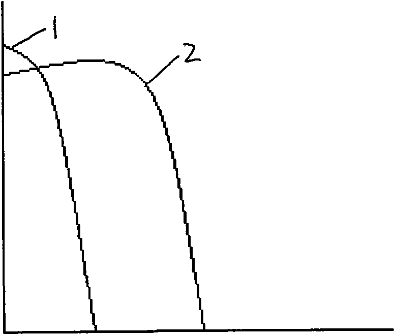
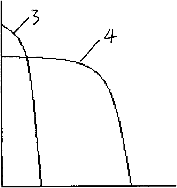
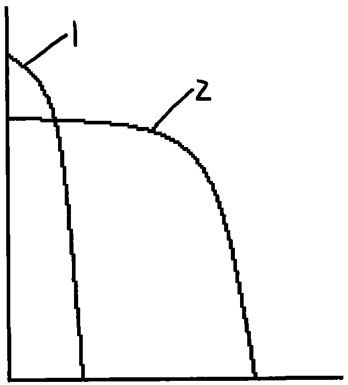
Increase the resistance of the current moving to the grid wire electrode in the emission area; and because the conduction between the electrode and the emission area depends on the tunneling effect, the contact resistance between the electrode and the emission area is also related to the doping amount. The higher the doping, the higher the contact resistance. Small; if the doping is too low, the contact resistance will increase rapidly, and even ohmic contact cannot be formed
[0004] As mentioned above, the doping concentration of the emitter region must take into account the above two requirements. The currently widely used process is usually selected at one temperature, and the temperature remains unchanged during the diffusion process. Considering the above requirements, a compromise t

Method used


Image

  • Diffusion method used for crystalline silicon solar battery
  • Diffusion method used for crystalline silicon solar battery
  • Diffusion method used for crystalline silicon solar battery

Examples


Embodiment 1

[0014] Embodiment 1: This embodiment includes the following steps: 1. Put the silicon wafer into the diffusion furnace for 10 minutes. 2. Raise the temperature from 810°C to 840°C, and feed POCL at the same time 3 700sccm, O 2 200sccm, N 2 6slm, with 12min. +The temperature gradient rises in the application of temperature rise and diffusion, which increases the activity of phosphorus atoms on the surface of the silicon body, making the phosphorus atoms that enter the silicon body have stronger activity, and increases the uniformity of phosphorus diffusion on silicon wafers. 3. Stabilize at 840°C for 2 minutes, while passing O 2 300sccm,N 2 6slm. 4. Raise the temperature from 840°C to 870°C, and feed POCL at the same time 3 500sccm, O 2 300sccm, N 2 6slm, time 8min. 5. Decrease the temperature from 870°C to 800°C, and pass O at the same time 2 500sccm, N 2 6slm; the combination of cooling promotion and gettering greatly shortens the process time and improves...

Embodiment 2

[0015] Embodiment 2: This embodiment includes the following steps: 1. Put the silicon wafer into the diffusion furnace. 2. Raise the temperature from 780°C to 850°C, and feed POCL at the same time 3 1000sccm, O 2 500sccm, N 2 8slm, it took 13min. 3. Stable at 850°C for 3 minutes, while passing O 2 400sccm,N 2 9slm. 4. Raise the temperature from 850°C to 880°C, and feed POCL at the same time 3 700sccm, O 2 500sccm, N 2 8slm, with 9min. 5. Decrease the temperature from 880°C to 800°C, and pass O at the same time 2 800sccm, N 2 9slm. 6. Stabilize at 800°C for 2 minutes, and pass POCL at the same time 3 2000sccm, O 2 800sccm, N 2 10slm. 7. Take out the silicon wafer from the diffusion furnace.

Embodiment 3

[0016] Embodiment 3: This embodiment includes the following steps: 1. Put the silicon wafer into the diffusion furnace. 2. Raise the temperature from 790°C to 860°C, and feed POCL at the same time 3 600sccm, O 2 300sccm, N 2 5slm, it takes 14min. 3. Stable at 860°C for 5 minutes, while passing O 2 200 sccm, N 2 5slm. 4. Raise the temperature from 860°C to 890°C, and feed POCL at the same time 3 600sccm, O 2 200sccm, N 2 5slm, with 12min. 5. Decrease the temperature from 890°C to 800°C, and pass O at the same time 2 300sccm, N 2 5slm. 6. Stabilize at 800°C for 2 minutes, and pass POCL at the same time 3 800sccm, O 2 1000sccm, N 2 12slm. 7. Take out the silicon wafer from the diffusion furnace.


PUM


Abstract

The invention discloses a diffusion method used for a crystalline silicon solar battery. The method comprises the following steps of: (1) placing a silicon wafer into a diffusion furnace; rising the temperature from 780-810 DEG C to 840-860 DEG C; and simultaneously introducing POCL3+O2+N2 for 12 to 14 minutes; (2) simultaneously introducing O2+N2 when rising the temperature in the diffusion furnace to 840-860 DEG C and keeping the constant temperature for 2 to 5 minutes; simultaneously introducing the POCL3+O2+N2 for 8 to 12 minutes when rising the temperature from 840-860 DEG C to 870-890 DEG C; reducing the temperature from 870-890 DEG C to 800 DEG C; introducing the O2+N2 in the process of reducing the temperature; stabilizing for 2 minutes at the temperature of 800 DEG C; and introducing the POCL3+O2+N2; and (3) taking the silicon wafer out of the diffusion furnace. In the method, both the requirements on the doping concentration of an emitting region and the surface concentration of the emitting region in diffusion can be met at the same time; a gettering effect is good; and the distribution of a doping curve is more reasonable.

Description

technical field [0001] The invention relates to a diffusion method, in particular to a diffusion method applied to crystalline silicon solar cells. Background technique [0002] Diffusion technology is the most important process of monocrystalline silicon and polycrystalline silicon solar cells. Its purpose is to form an emitter region with the conductivity type opposite to that of the substrate, thereby forming a PN junction. Usually monocrystalline silicon and polycrystalline silicon solar cells use P-type substrates, phosphorus oxychloride POCL 3 Liquid source diffusion forms a phosphorous-doped N-type emission region through a series of chemical reactions and phosphorus atom diffusion processes. Generally, the diffusion temperature is set at 830-870°C and the source time is 20-35 minutes; during the high temperature process, POCL 3 Nitrogen (generally called this part of nitrogen as small nitrogen) is carried into the quartz tube, and nitrogen (generally called this par...

Claims


Application Information

Patent Timeline
IPC IPC(8): H01L31/18C30B31/08
CPCY02P70/50
Inventor 俆英乾
Owner BAODING GUANGWEI GREEN ENERGY TECH CO LTD
Why Eureka
Try Eureka