Multi-layer composite passivation layer structure of bipolar circuit and its production process

A multi-layer composite and generation process technology, applied in the direction of circuits, electrical components, electrical solid devices, etc., can solve the problems of limited application, poor photoelectric performance, and poor step coverage ability, so as to improve the small current amplification factor and avoid stress migration , improve the effect of linearity

Inactive Publication Date: 2011-12-14
HANGZHOU SILAN INTEGRATED CIRCUIT
View PDF0 Cites 0 Cited by
  • Summary
  • Abstract
  • Description
  • Claims
  • Application Information

AI Technical Summary

Problems solved by technology

However, due to the shortcomings of silicon oxide such as radiation sensitivity, low scratch resistance, poor photoelectric performance, weak moisture resistance and mobile ion penetration, it is limited in special semiconductor processes and devices (such as silicon photoelectric conversion circuits, etc.)
For the silicon oxide film formed by the conventional low-pressure chemical vapor deposition method, due to its better step conformality, in the double-layer wiring process without planarization process, the passivation film is between the vertical edge and the surface parallel to the layer. Gaps are prone to appear at the corners of high steps, which weakens the protective effect of the silicon oxide passivation film here, thereby affecting the thermal stability and reliability of the circuit
Silicon nitride is another commonly used passivation layer dielectric material. Its barrier effect on mobile ions and water vapor is the best among all commonly used dielectric materials, and it has high scratch resistance. However, silicon nitride material The step coverage ability of the aluminum alloy is poor, and it is prone to breakage at high steps without a planarization process. At the same time, its expansion coefficient is greatly different from that of aluminum materials, and it is easy to deform after high temperature annealing

Method used


Image

  • Multi-layer composite passivation layer structure of bipolar circuit and its production process
  • Multi-layer composite passivation layer structure of bipolar circuit and its production process
  • Multi-layer composite passivation layer structure of bipolar circuit and its production process

Examples


Embodiment Construction

[0019] The content of the present invention will be further described below with reference to the accompanying drawings and taking a photoelectric conversion integrated circuit as an embodiment.

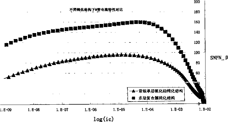
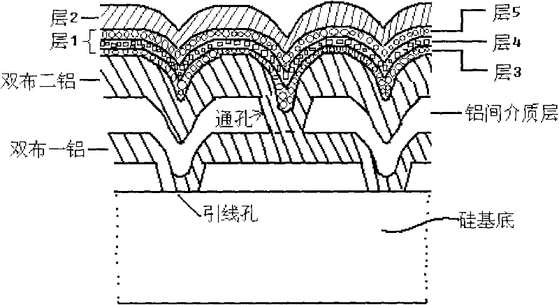
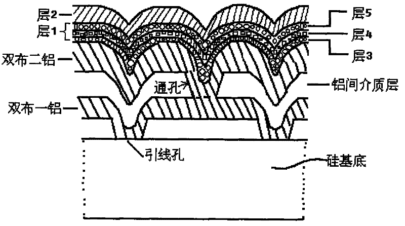
[0020] The multilayer composite passivation film structure of Bipolar circuit, such as figure 1 As shown, it includes a bottom silicon oxide thin film layer (1) deposited on the silicon substrate surface and a silicon nitride thin film layer (2) deposited on the silicon oxide thin film layer (1), and the silicon oxide thin film layer ( 1) is mixed with a certain proportion of phosphine, and the proportion of phosphine in the silicon oxide film layer is 3% to 5%, and the silicon oxide film layer (1) is followed by an undoped silicon dioxide layer (3), doped impurity phosphosilicate glass layer (4), non-doped silicon dioxide layer (5), the silicon substrate surface has double cloth-aluminum, aluminum interlayer dielectric layer, double cloth two aluminum. Among them, the silicon nitri...


PUM


Abstract

The present invention provides the multilayer composite passivation film structure of the Bipolar circuit, comprising the underlying silicon oxide film layer deposited on the surface of the silicon substrate and the silicon nitride film layer deposited on the silicon oxide film layer, the silicon oxide film layer A certain proportion of phosphine is doped in the layer, and the silicon oxide film layer is an undoped silicon dioxide layer, a doped phosphosilicate glass layer, and an undoped silicon dioxide layer in sequence. Simultaneously, the present invention also provides the multilayer composite passivation film production method of Bipolar circuit, utilizes the multilayer composite passivation film structure of Bipolar circuit realized by the present invention to have anti-scratch, anti-moisture, high density, low film stress, Higher gettering ability, better step coverage ability, excellent photoelectric performance, electrical characteristics and thermal stability, reducing soft breakdown and solving problems such as poor reliability.

Description

technical field [0001] The invention relates to a passivation layer structure and a passivation layer generation process in the field of semiconductor manufacturing, in particular to a multilayer composite passivation layer structure of a Bipolar circuit and a generation process method thereof. Background technique [0002] Silicon oxide is widely used as a conventional passivation film structure in BiDolar circuits due to its relatively small stress on the silicon substrate and aluminum film. However, due to the shortcomings of silicon oxide such as radiation sensitivity, low scratch resistance, poor photoelectric performance, weak moisture resistance and mobile ion penetration, it is limited in special semiconductor processes and devices (such as silicon photoelectric application in conversion circuits, etc.). For the silicon oxide film formed by the conventional low-pressure chemical vapor deposition method, due to its better step conformality, in the double-layer wiring...

Claims


Application Information

Patent Timeline
Patent Type & Authority Patents(China)
IPC IPC(8): H01L23/00H01L21/314H01L21/3105
Inventor 刘琛李小锋吕艳欣陈元金
Owner HANGZHOU SILAN INTEGRATED CIRCUIT
Why Eureka
Try Eureka