Method for manufacturing semiconductor epitaxial wafer, method for manufacturing semiconductor epitaxial wafer, and solid-state imaging device

A technology of solid-state imaging elements and epitaxial wafers, which is applied in semiconductor/solid-state device manufacturing, semiconductor devices, electric solid-state devices, etc., and can solve problems such as insufficiency

Active Publication Date: 2017-09-08
SUMCO CORP
View PDF14 Cites 0 Cited by
  • Summary
  • Abstract
  • Description
  • Claims
  • Application Information

AI Technical Summary

Problems solved by technology

In recent years, these metal contaminations have been improved to some extent by changing the constituent materials of the epitaxial growth furnace to materials with excellent corrosion resistance, etc., but this is not enough.

Method used


Image

  • Method for manufacturing semiconductor epitaxial wafer, method for manufacturing semiconductor epitaxial wafer, and solid-state imaging device
  • Method for manufacturing semiconductor epitaxial wafer, method for manufacturing semiconductor epitaxial wafer, and solid-state imaging device
  • Method for manufacturing semiconductor epitaxial wafer, method for manufacturing semiconductor epitaxial wafer, and solid-state imaging device

Examples


Embodiment

[0081] (Refer to the experimental example)

[0082] First, in order to clarify the difference between cluster ion irradiation and monomer ion implantation, the following experiments were performed.

reference example 1)

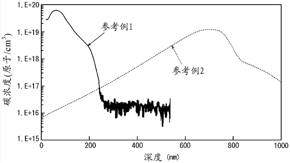
[0084] An n-type silicon wafer (diameter: 300 mm, thickness: 725 μm, doping: phosphorus, doping concentration: 4×10 14 atom / cm 3 ). Next, use a cluster ion generator (manufactured by Nisshin Ion Equipment Co., Ltd., model: CLARIS) to pass through biphenyl (C 14 h 14 ) to generate C 5 h 5 clusters, at a dose of 1.2 x 10 14 Cluster / cm 2 (Carbon dosage 6.0 x 10 14 atom / cm 2 ), the silicon wafer was irradiated under the irradiation conditions of 14.8keV / atom per carbon atom.

reference example 2)

[0086] For the same silicon wafer as in Reference Example 1, instead of cluster ion irradiation, CO 2 As a material gas, carbon monomer ions are generated, and the dose is set to 1.2×10 14 atom / cm 2 The silicon wafer was irradiated under the same conditions as in Reference Example 1 except for the conditions of an accelerating voltage of 300 keV / atom.

[0087] (SIMS measurement result)

[0088] The samples prepared in the above reference examples 1 and 2 were measured by SIMS to obtain Figure 4 Concentration profiles of carbon are shown. In addition, the depth of the horizontal axis is zero from the surface of the silicon wafer. if according to the Figure 4 As is apparent, in Reference Example 1 in which cluster ion irradiation was performed, the carbon concentration distribution was sharp, whereas in Reference Example 2 in which monomer ion implantation was performed, the carbon concentration distribution was broad. In addition, compared with Reference Example 2, in R...


PUM

PropertyMeasurementUnit
hazeaaaaaaaaaa
widthaaaaaaaaaa
thicknessaaaaaaaaaa

Abstract

The object is to provide a method of manufacturing a semiconductor epitaxial wafer having a higher gettering capability and a reduced haze level of the surface of the epitaxial layer. The method for manufacturing a semiconductor epitaxial wafer according to the present invention is characterized in that it includes a first step of irradiating the semiconductor wafer 10 with cluster ions 16 to form a modified layer made of constituent elements of the cluster ions 16 on the surface 10A of the semiconductor wafer. 18. In the second step, after the first step, the semiconductor wafer 10 is subjected to heat treatment for crystallinity recovery in such a manner that the haze level of the semiconductor wafer surface 10A becomes 0.20 ppm or less; and in the third step, in the second step, After the process, an epitaxial layer 20 is formed on the modified layer 18 of the semiconductor wafer.

Description

technical field [0001] The present invention relates to a method for manufacturing a semiconductor epitaxial wafer, a method for manufacturing a semiconductor epitaxial wafer, and a solid-state imaging device. In particular, the present invention relates to a method of manufacturing a semiconductor epitaxial wafer capable of suppressing metal contamination by exerting a higher gettering capability and reducing the haze level of the surface of the epitaxial layer. Background technique [0002] Metal contamination is mentioned as a factor that degrades the characteristics of semiconductor devices. For example, in a back-illuminated solid-state imaging device, metal mixed into a semiconductor epitaxial wafer serving as a substrate of the device causes an increase in dark current of the solid-state imaging device, causing a defect called a white damage defect. The back-illuminated solid-state imaging device can directly introduce light from the outside to the sensor by arrangin...

Claims


Application Information

Patent Timeline
Patent Type & Authority Patents(China)
IPC IPC(8): H01L21/322C23C16/02C23C16/24C30B25/20H01L21/20H01L21/205H01L21/265H01L27/14
CPCH01L27/14689H01L21/02381H01L21/02439H01L21/02532H01L21/02576H01L21/02579H01L21/02658H01L21/26506H01L21/26513H01L21/26566H01L21/3221H01L27/14683C23C16/0209C23C16/0263C23C16/24C30B25/20H01L21/2658H01L27/14687C23C14/48H01L21/265H01L21/322
Inventor 门野武栗田一成
Owner SUMCO CORP
Why Eureka
Try Eureka