A kind of preparation method of crystalline silicon solar cell

A technology of solar cells and crystalline silicon, applied in the field of solar cells, can solve the problems such as the inability to achieve phosphorus gettering on the back of silicon wafers, and achieve the effects of improving cell conversion efficiency, improving gettering effects, and increasing production capacity

Active Publication Date: 2016-01-20
CHINT NEW ENERGY TECH (HAINING) CO LTD
View PDF4 Cites 0 Cited by
  • Summary
  • Abstract
  • Description
  • Claims
  • Application Information

AI Technical Summary

Problems solved by technology

[0006] In order to solve the problem that phosphorus gettering on the back of the silicon wafer cannot be achieved when high-quality p-n junctions are prepared by ion implantation technology, the present invention adopts single-side diffusion technology to diffuse high-concentration phosphorus on the back of the silicon wafer to realize the phosphorous gettering on the back of the silicon wafer. Getter

Method used


Image

  • A kind of preparation method of crystalline silicon solar cell
  • A kind of preparation method of crystalline silicon solar cell
  • A kind of preparation method of crystalline silicon solar cell

Examples


Embodiment Construction

[0021] The following disclosure provides many different embodiments or examples for implementing different structures of the present invention. To simplify the disclosure of the present invention, components and arrangements of specific examples are described below. Furthermore, the present invention may repeat reference numerals and / or letters in different instances. This repetition is for the purpose of simplicity and clarity and does not in itself indicate a relationship between the various embodiments and / or arrangements discussed. It should be noted that components illustrated in the figures are not necessarily drawn to scale. Descriptions of well-known components and processing techniques and processes are omitted herein to avoid unnecessarily limiting the present invention.

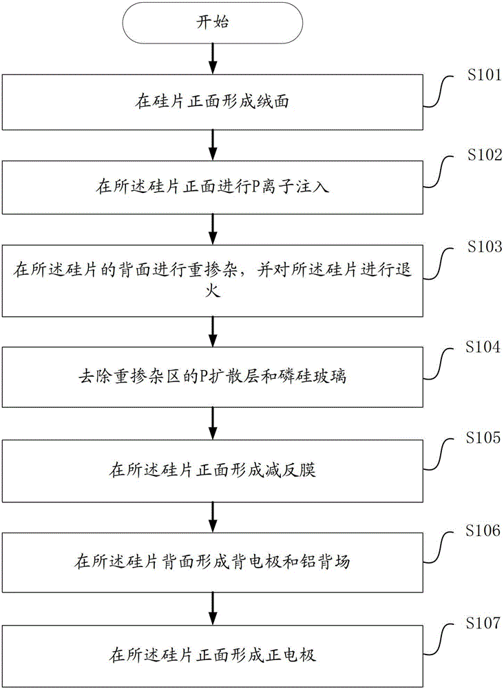
[0022] refer to figure 1 , figure 1 Shown is a schematic flow chart of a specific embodiment of a method for preparing a crystalline silicon solar cell according to the present invention.

[0...


PUM


Abstract

The invention discloses a method for preparing a crystalline silicon solar cell. The method comprises the following steps of: forming suede on the front surface of a silicon wafer; performing P ion implantation on the front surface of the silicon wafer; performing heavy doping on the back surface of the silicon wafer, and annealing the silicon wafer; removing a P diffusion layer and phosphorosilicate glass from a heavy doping region; forming an anti-reflection film on the front surface of the silicon wafer; forming a back electrode and an aluminum back field on the back surface of the silicon wafer; and forming a front electrode on the front surface of the silicon wafer. The solar cell prepared by using the method has an efficient p-n junction which is obtained by ion implantation, and has a good back gettering effect; and photoelectric conversion efficiency is remarkably improved.

Description

technical field [0001] The invention relates to the technical field of solar cells, in particular to a method for preparing a p-n junction crystalline silicon solar cell by means of ion implantation. Background technique [0002] The core part of the crystalline silicon solar cell is the p-n junction. In the prior art, POCl3 thermal diffusion is usually used to diffuse P into the silicon wafer to obtain the p-n junction. However, it is difficult to control the doping concentration during the implementation of the above method, and the depth uniformity of the p-n junction is not good, so it is difficult to improve the photoelectric conversion efficiency of the solar cell. Ion implantation technology can implant various doping substances into the base material, and can also achieve precise control over the depth and concentration of the implantation. Therefore, many companies have applied ion implantation technology to the preparation process of crystalline silicon solar cell...

Claims


Application Information

Patent Timeline
Patent Type & Authority Patents(China)
IPC IPC(8): H01L31/18
CPCY02P70/50
Inventor 石强李旺单伟韩玮智牛新伟蒋前哨金建波仇展炜
Owner CHINT NEW ENERGY TECH (HAINING) CO LTD
Why Eureka
Try Eureka