Schottky diode and manufacturing method thereof

A Schottky diode and Schottky contact technology, applied in semiconductor/solid-state device manufacturing, electrical components, circuits, etc., can solve the problem of not fully utilizing the voltage resistance potential of the overall epitaxial layer, the current transmission capacity has a greater impact, and increase stability. The difficulty of maintaining stability and other issues can achieve the effects of good current transmission capacity and stability, low production cost, and reduced performance impact.

Active Publication Date: 2015-05-13
FIFTH ELECTRONICS RES INST OF MINIST OF IND & INFORMATION TECH
View PDF6 Cites 14 Cited by
  • Summary
  • Abstract
  • Description
  • Claims
  • Application Information

AI Technical Summary

Problems solved by technology

[0010] First of all, the existing field plate structure, guard ring structure or super junction structure, because they are very close to the GaN heterojunction active region, and are usually fabricated by field plate technology and ion implantation technology, have an impact on the current transmission capability of the device. Larger, while improving the withstand voltage performance, it sacrifices the larger output characteristics of the device;
[0011] Secondly, these technical means do not make full use of the voltage-resistant potential of the overall epitaxial layer, and the space for further improvement of the voltage-resistant performance is very limited;
[0012] Thirdly, whether it is the field plate process or the ion implantation process, it increases the difficulty of maintaining stability in the device manufacturing process, and also increases the manufacturing cost of the device, which is not conducive to the promotion of industrialization

Method used


Image

  • Schottky diode and manufacturing method thereof
  • Schottky diode and manufacturing method thereof
  • Schottky diode and manufacturing method thereof

Examples


Embodiment

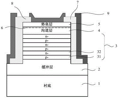
[0061] In this embodiment, a Schottky diode, such as image 3 As shown, it includes: a substrate 1, a buffer layer 2, an epitaxial structure, a Schottky contact metal 7, and an ohmic contact metal 8, and the substrate 1, the buffer layer 2, and the epitaxial structure are sequentially stacked;

[0062] The epitaxial structure includes a superjunction layer 3, a GaN channel layer 4 and a barrier layer 5 stacked in sequence, and the superjunction layer 3 is formed by alternately stacking a plurality of p-type GaN layers 31 and n-type GaN layers 32;

[0063] The Schottky contact metal 7 and the ohmic contact metal 8 are respectively symmetrically disposed on opposite side surfaces of the epitaxial structure, and one end extends to the upper surface of the epitaxial structure, and the other end extends to the buffer layer 2 .

[0064] In the Schottky diode, the Schottky contact metal 7 and the ohmic contact metal 8 are respectively arranged symmetrically on opposite sides of the e...


PUM

PropertyMeasurementUnit
thicknessaaaaaaaaaa
thicknessaaaaaaaaaa
thicknessaaaaaaaaaa

Abstract

The invention discloses a Schottky diode and a manufacturing method thereof. The Schottky diode comprises a substrate, a buffer layer, an extension structure, a Schottky contact metal and an Ohmic contact metal, wherein the substrate the buffer layer and the extension structure are sequentially arranged in an overlapped structure; the extension structure comprises a super bonding layer, a GaN channel layer and a barrier layer which are sequentially stacked, and the super bonding layer is composed of a plurality of p-type GaN layer and a plurality of n-type GaN layer which are alternately stacked each other; the Schottky contact metal and the Ohmic contact metal are symmetrically arranged on the opposite two side surfaces of the extension structure, one ends of the Schottky contact metal and the Ohmic contact metal extend to the upper surface of the extension structure, and the other ends of the Schottky contact metal and the Ohmic contact metal extend to the buffer layer. The Schottky diode has relatively high pressure resistance, ensures current transmission capacity and stability and avoids a traditional field plate structure or protecting ring structure, thereby simplifying the manufacturing process and reducing the cost.

Description

technical field [0001] The invention relates to a semiconductor device, in particular to a Schottky diode and a manufacturing method thereof. Background technique [0002] In modern society, power electronics technology continues to update and develop, and power electronic devices such as voltage regulators, rectifiers, and inverters are more and more widely used in daily life, involving high-voltage power supply, power management, factory automation, and energy distribution management for motor vehicles. Many fields. [0003] Diodes are an integral part of power electronics applications. In recent years, Schottky diodes with high frequency, high current and low power consumption have attracted more and more attention due to their unique performance advantages. [0004] Traditional power Schottky diodes are mainly fabricated on silicon (Si)-based materials. The development of silicon materials has a long history, the cost of silicon single crystal preparation is low, and ...

Claims


Application Information

Patent Timeline
Patent Type & Authority Applications(China)
IPC IPC(8): H01L29/872H01L29/16H01L21/329H01L29/06
CPCH01L29/0603H01L29/0684H01L29/16H01L29/66143H01L29/872H01L29/0634H01L29/2003H01L29/205
Inventor 贺致远徐华伟黄庆礼黄林轶
Owner FIFTH ELECTRONICS RES INST OF MINIST OF IND & INFORMATION TECH
Why Eureka
Try Eureka