Method for manufacturing nitride semiconductor light-emitting element

a technology of semiconductor light-emitting elements and manufacturing methods, which is applied in semiconductor devices, semiconductor lasers, lasers, etc., can solve the problems of difficult to obtain acceptable products stably throughout the entire surface of the wafer, difficult to stably obtain contact resistivity, and resulted in p-type electrode degradation, etc., to achieve low production cost, low time degradation, and low production cost

Inactive Publication Date: 2009-05-21
MITSUBISHI ELECTRIC CORP
View PDF14 Cites 5 Cited by
  • Summary
  • Abstract
  • Description
  • Claims
  • Application Information

AI Technical Summary

Benefits of technology

[0013]According to the present invention, the contact resistivity of a p-type electrode can be lowered. As a result, a long-life laser diode capable of high-output operation with little time degradation can be obtained. Also by performing electrode metal vapor deposition prior to the insulating film forming process, electrode peeling can be suppressed, and a long-life laser diode capable of high-output operation with little time degradation can be obtained at high yield.

Problems solved by technology

Heretofore, it was difficult to stably obtain contact resistivity lower than 1E-3 Ωcm2 in the p-type electrode throughout the entire surface of the wafer.
Therefore, when a nitride semiconductor light-emitting element was operated especially by a laser diode at an optical output of 200 mW or higher, degradation caused by the p-type electrode was resulted.
Therefore, it was difficult to obtain acceptable products stably throughout the entire surface of the wafer.

Method used


Image

  • Method for manufacturing nitride semiconductor light-emitting element
  • Method for manufacturing nitride semiconductor light-emitting element
  • Method for manufacturing nitride semiconductor light-emitting element

Examples


embodiment 1

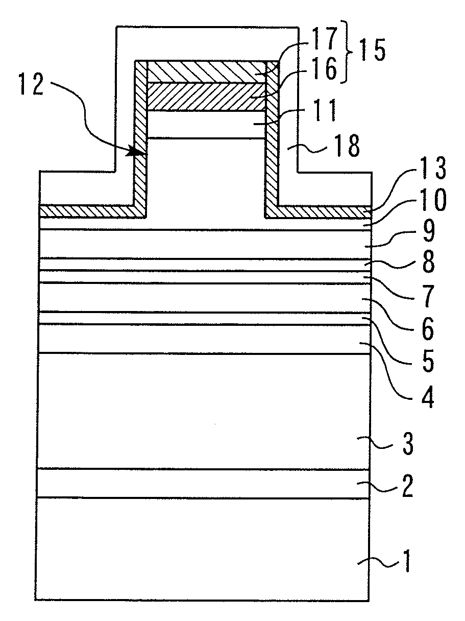
[0021]FIG. 1 is a sectional view showing a nitride semiconductor laser diode according to the Embodiment 1. An n-type GaN buffer layer 2 is formed on the GaN surface, which is a major surface of a GaN substrate 1 (substrate). The n-type GaN buffer layer 2 is formed to reduce the irregularity of the surface of the GaN substrate 1 and to laminate upper layers as flatly as possible. An n-type AlGaN clad layer 3 is formed on the n-type GaN buffer layer 2.

[0022]On the n-type AlGaN clad layer 3, an n-type GaN light-guide layer 4 and an undoped InGaN light-guide layer 5 are sequentially laminated. On the InGaN light-guide layer 5, an active layer 6 having an undoped InxGa1-xN / InyGa1-yN(0

[0023]On the active layer 6, an undoped InxGa1-xN(07 as a p-side light-guide layer, a p-type AlGaN electron barrier layer 8, a p-type GaN light-guide layer 9 as a p-side light-guide layer, a p-type AlGaN clad layer 10, and a p-type GaN contact layer 11 (p-t...

embodiment 2

[0053]Next, the method for manufacturing a nitride semiconductor light-emitting element according to the Embodiment 2 will be described.

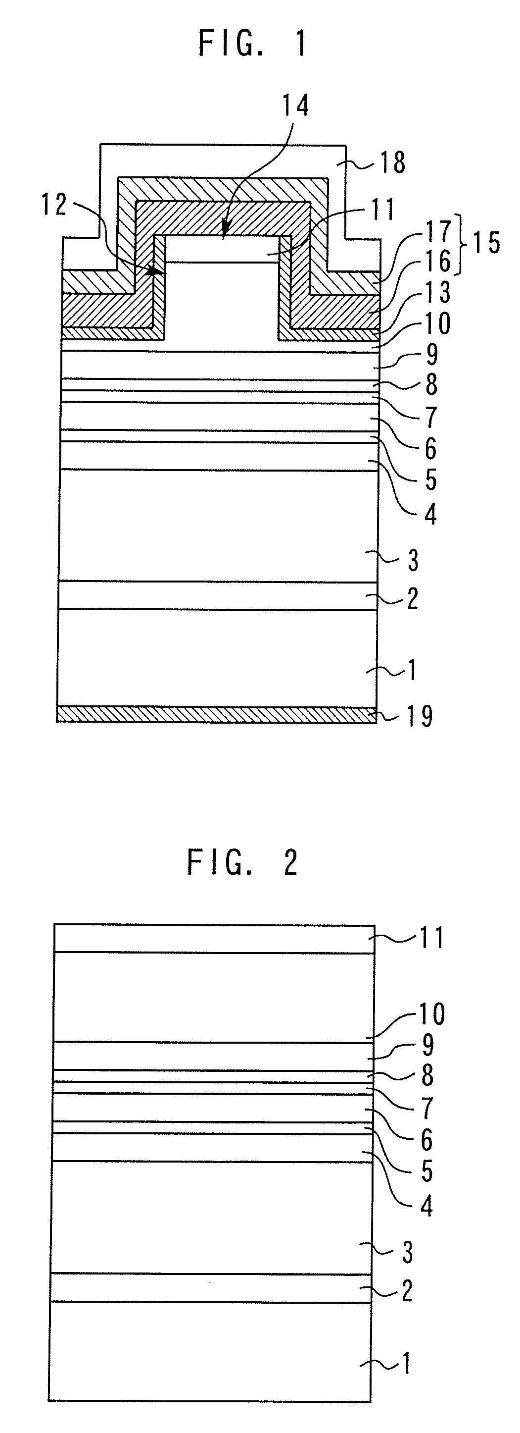
[0054]First, as shown in FIG. 2, on a GaN substrate 1, a nitride semiconductor epitaxial layer is formed in the same manner as in the Embodiment 1.

[0055]Next, as shown in FIG. 14, a Pd layer 16 and a Ta layer 17 are sequentially formed by electron beam (EB) vapor deposition and lift off as a p-type electrode 15.

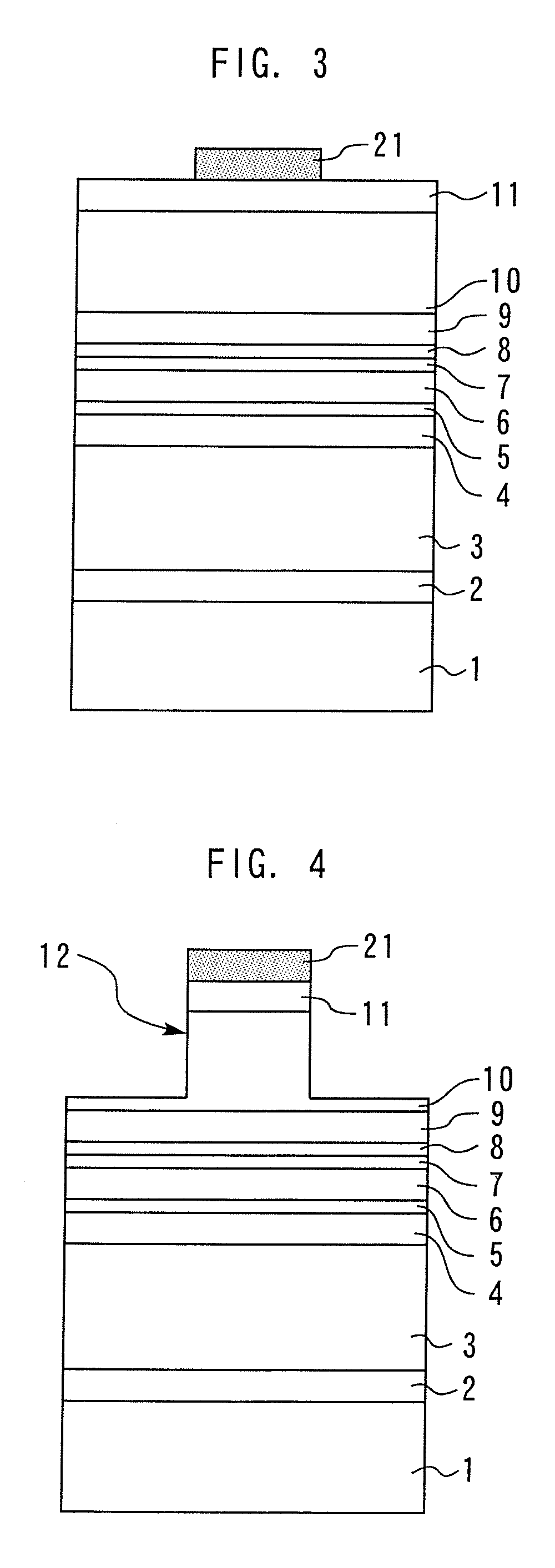
[0056]Next, as shown in FIG. 15, a resist is applied onto the entire surface of the wafer subjected to the above-described crystal growth, and a resist pattern 21 having a predetermined shape is formed by lithography (photoengraving).

[0057]Next, as shown in FIG. 16, the p-type electrode 15 and the p-type nitride semiconductor epitaxial layers are subjected to anisotropic etching to the inside of the p-type AlGaN clad layer 10 by RIE or the like using the resist pattern 21 as a mask to form a ridge 12, which becomes a waveguide structure. As t...


PUM

PropertyMeasurementUnit
temperatureaaaaaaaaaa

Abstract

A method for manufacturing a nitride semiconductor light-emitting element comprises: forming a semiconductor laminated structure wherein an n-type nitride semiconductor epitaxial layer, an active layer, and a p-type nitride semiconductor epitaxial layer are laminated on a substrate; forming a p-type electrode having a first electrode layer containing Pd and a second electrode layer containing Ta on the p-type nitride semiconductor epitaxial layer; heat treating at a temperature between 400° C. and 600° C. in an ambient containing oxygen after forming the p-type electrode; and forming a pad electrode containing Au on the p-type electrode after the heat treating.

Description

BACKGROUND OF THE INVENTION[0001]1. Field of the Invention[0002]The present invention relates to a method for manufacturing a nitride semiconductor light-emitting element wherein a p-type electrode is formed on a p-type nitride semiconductor epitaxial layer. More specifically, the present invention relates to a method for manufacturing a nitride semiconductor light-emitting element that can reduce the contact resistivity of a p-type electrode.[0003]2. Background Art[0004]When a high-output operation exceeding 200 mW is performed by a nitride semiconductor light-emitting element, the elevation of operating voltage causes a problem in the long burn-in test. To solve such a problem, a p-type electrode having a low resistance and uniform contact characteristics is required. As an electrode material that satisfies such requirement, Pd, that has a large work function is promising.[0005]As the method for forming an electrode containing Pd as the major component on the surface of a nitride ...

Claims


Application Information

Patent Timeline
Patent Type & Authority Applications(United States)
IPC IPC(8): H01L21/20H01S5/042H01S5/343
CPCB82Y20/00H01L33/32H01L33/40H01S5/0021H01S5/0425H01S2304/04H01S5/22H01S5/3213H01S5/34333H01S2301/173H01S5/2009H01S5/04252
Inventor KANAMOTO, KYOZOSHIOZAWA, KATSUOMIKAWASAKI, KAZUSHIGEABE, SHINJISAKUMA, HITOSHI
Owner MITSUBISHI ELECTRIC CORP
Why Eureka
Try Eureka