Method for manufacturing nitride semiconductor light-emitting element
a technology of semiconductor light-emitting elements and manufacturing methods, which is applied in semiconductor devices, semiconductor lasers, lasers, etc., can solve the problems of difficult to obtain acceptable products stably throughout the entire surface of the wafer, difficult to stably obtain contact resistivity, and resulted in p-type electrode degradation, etc., to achieve low production cost, low time degradation, and low production cost
- Summary
- Abstract
- Description
- Claims
- Application Information
AI Technical Summary
Benefits of technology
Problems solved by technology
Method used
Image
Examples
embodiment 1
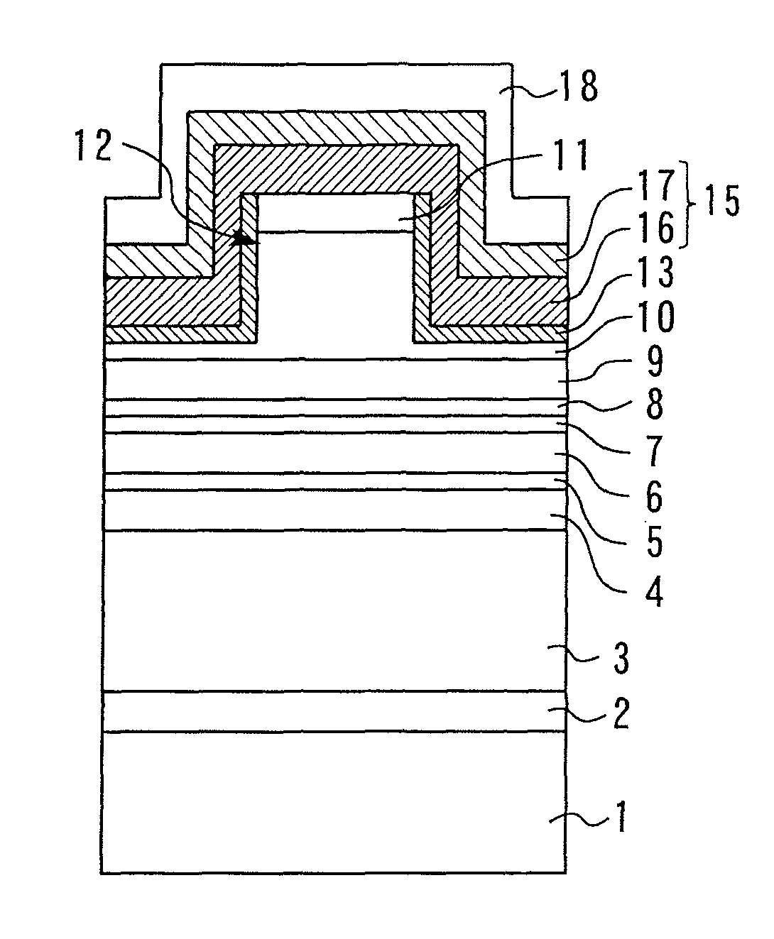
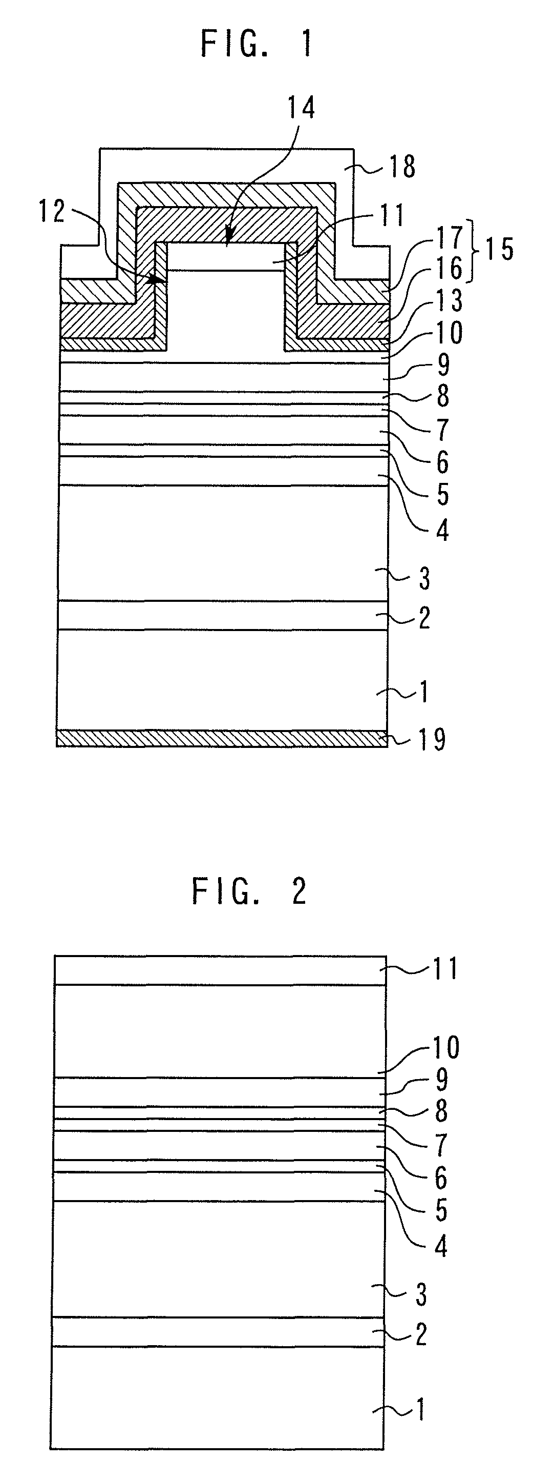
[0021]FIG. 1 is a sectional view showing a nitride semiconductor laser diode according to the Embodiment 1. An n-type GaN buffer layer 2 is formed on the GaN surface, which is a major surface of a GaN substrate 1 (substrate). The n-type GaN buffer layer 2 is formed to reduce the irregularity of the surface of the GaN substrate 1 and to laminate upper layers as flatly as possible. An n-type AlGaN clad layer 3 is formed on the n-type GaN buffer layer 2.
[0022]On the n-type AlGaN clad layer 3, an n-type GaN light-guide layer 4 and an undoped InGaN light-guide layer 5 are sequentially laminated. On the InGaN light-guide layer 5, an active layer 6 having an undoped InxGa1-xN / InyGa1-yN (0<x, y<1) multiple quantum well structure is formed.
[0023]On the active layer 6, an undoped InxGa1-xN (07 as a p-side light-guide layer, a p-type AlGaN electron barrier layer 8, a p-type GaN light-guide layer 9 as a p-side light-guide layer, a p-type AlGaN clad layer 10, and a p-type GaN contact layer 11 (p...
embodiment 2
[0053]Next, the method for manufacturing a nitride semiconductor light-emitting element according to the Embodiment 2 will be described.
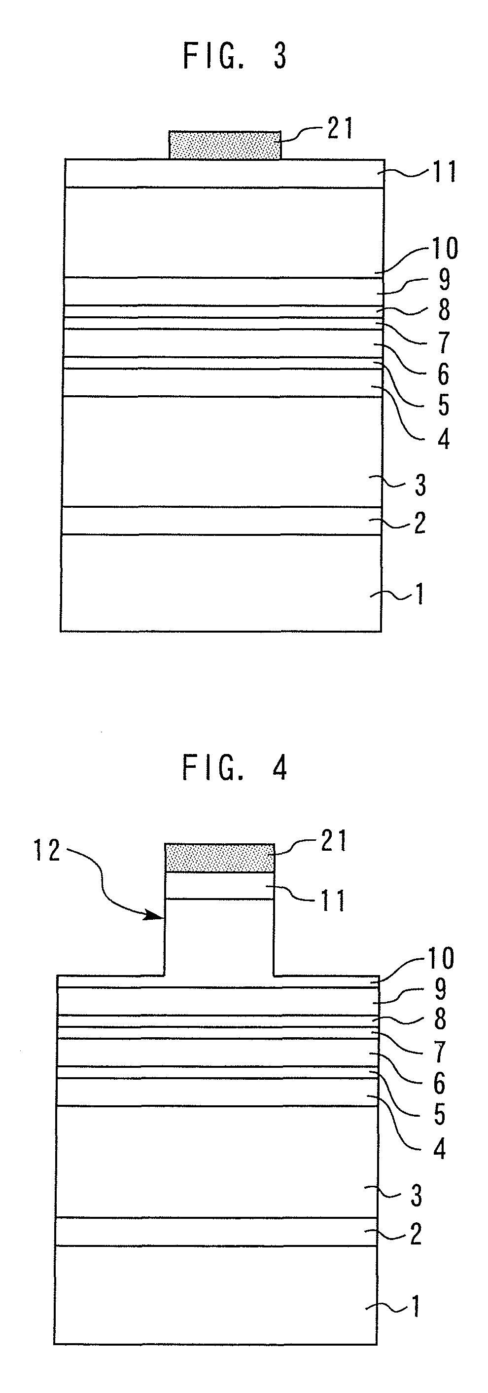
[0054]First, as shown in FIG. 2, on a GaN substrate 1, a nitride semiconductor epitaxial layer is formed in the same manner as in the Embodiment 1.
[0055]Next, as shown in FIG. 14, a Pd layer 16 and a Ta layer 17 are sequentially formed by electron beam (EB) vapor deposition and lift off as a p-type electrode 15.
[0056]Next, as shown in FIG. 15, a resist is applied onto the entire surface of the wafer subjected to the above-described crystal growth, and a resist pattern 21 having a predetermined shape is formed by lithography (photoengraving).
[0057]Next, as shown in FIG. 16, the p-type electrode 15 and the p-type nitride semiconductor epitaxial layers are subjected to anisotropic etching to the inside of the p-type AlGaN clad layer 10 by RIE or the like using the resist pattern 21 as a mask to form a ridge 12, which becomes a waveguide structure. As t...
PUM
| Property | Measurement | Unit |
|---|---|---|
| temperature | aaaaa | aaaaa |
| temperature | aaaaa | aaaaa |
| temperature | aaaaa | aaaaa |
Abstract
Description
Claims
Application Information


