Method for reducing Ohmic contact resistivity of gallium nitride high electron mobility transistor

A technology with high electron mobility and ohmic contact, applied in circuits, electrical components, semiconductor devices, etc., can solve problems such as difficult ohmic contact resistance, achieve good process implantability, improve device performance, and improve device performance Effect

Inactive Publication Date: 2016-11-02
CHENGDU HIWAFER SEMICON CO LTD
View PDF3 Cites 5 Cited by
  • Summary
  • Abstract
  • Description
  • Claims
  • Application Information

AI Technical Summary

Problems solved by technology

[0004] The main disadvantage of the current ohmic contact manufacturing method is that the optimization of ohmic contact resistivity is mainly obtained by adjusting the metal thickness of each layer and annealing conditions, but the ohmic contact resistance obtained by this technology is difficult to achieve 0.5Ω·mm the following

Method used


Image

  • Method for reducing Ohmic contact resistivity of gallium nitride high electron mobility transistor
  • Method for reducing Ohmic contact resistivity of gallium nitride high electron mobility transistor
  • Method for reducing Ohmic contact resistivity of gallium nitride high electron mobility transistor

Examples


Embodiment Construction

[0017] The following will clearly and completely describe the technical solutions in the embodiments of the present invention with reference to the accompanying drawings in the embodiments of the present invention. Obviously, the described embodiments are only some, not all, embodiments of the present invention. Based on the embodiments of the present invention, all other embodiments obtained by persons of ordinary skill in the art without making creative efforts belong to the protection scope of the present invention.

[0018] see figure 1 , is a schematic flowchart of a method for reducing the ohmic contact resistivity of a gallium nitride high electron mobility transistor according to an embodiment of the present invention. The method of the present embodiment comprises the following steps:

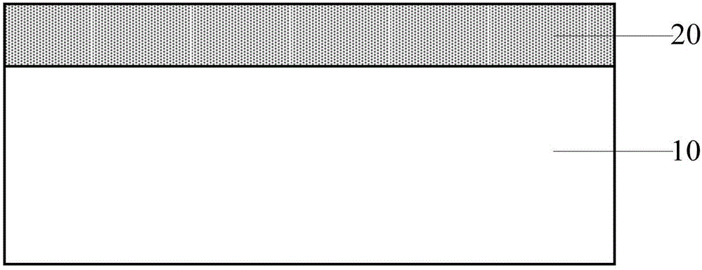
[0019] S11: Spin-coat photoresist on the surface of the wafer to form a photoresist layer.

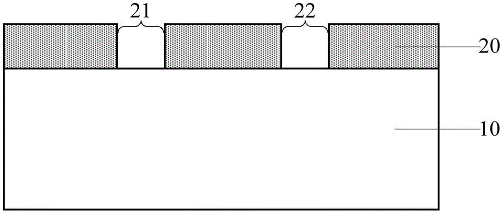
[0020] Among them, such as figure 2 As shown, a photoresist layer 20 is formed on the s...


PUM


Abstract

The invention provides a method for reducing Ohmic contact resistivity of a gallium nitride high electron mobility transistor. The method comprises the following steps: a photoresist layer is formed by coating photoresist on a wafer surface via spin coating operation, a source electrode area and a drain electrode area are etched on the photoresist layer via photoetching processes, and the source electrode area and the drain electrode area are exposed on the wafer surface; argon ions are sputtered on parts, positioned in the source electrode area and the drain electrode area, of the wafer surface; the argon ions are enabled to bombard the wafer surface; a source metal electrode and a drain metal electrode are formed by sputtering metal on the parts, positioned in the source electrode area and the drain electrode area, of the wafer surface; the photoresist layer is peeled off, and the source metal electrode and the drain metal electrode are enable to be in Ohmic contact with each other via adoption of high temperature rapid thermal annealing processes. Via the above mode, the method for reducing Ohmic contact resistivity of the gallium nitride high electron mobility transistor can help increase concentration of N vacancy in a semiconductor, and low Ohmic contact resistivity can be obtained via high temperature thermal annealing alloying technologies.

Description

technical field [0001] The invention relates to the technical field of semiconductor manufacturing, in particular to a method for reducing the ohmic contact resistivity of a gallium nitride high electron mobility transistor. Background technique [0002] GaN-based high electron mobility transistor (HEMT) has become the technology of choice for next-generation RF / microwave power amplifiers due to its unique high electron mobility, high two-dimensional electron gas surface density, and high breakdown electric field. The epitaxial layers of a typical GaN-based HEMT are not intentionally doped, and the barrier layer has a large band gap, so the preparation of the source-drain ohmic contact is much more difficult than GaAs and InPHEMT. [0003] A HEMT device has three electrode terminals in total: source, drain, and gate. Both the source electrode and the drain electrode need to form ohmic contact with the semiconductor material. The quality of the ohmic contact will largely det...

Claims


Application Information

Patent Timeline
Patent Type & Authority Applications(China)
IPC IPC(8): H01L21/335H01L21/28H01L21/02
CPCH01L29/66462H01L21/02071H01L21/28
Inventor 孔欣
Owner CHENGDU HIWAFER SEMICON CO LTD
Why Eureka
Try Eureka