p-type GaN epitaxial wafer with high ohmic contact features and preparation method thereof

A technology of ohmic contact and epitaxial wafers, applied in the structure of active regions, semiconductor/solid-state device manufacturing, electrical components, etc., can solve the problems of deteriorating p-type characteristics, low photoelectric conversion efficiency, heat generation, etc., to reduce the probability of degradation, Effect of improving electro-optic conversion efficiency

Inactive Publication Date: 2019-06-07
INST OF SEMICONDUCTORS - CHINESE ACAD OF SCI
View PDF8 Cites 6 Cited by
  • Summary
  • Abstract
  • Description
  • Claims
  • Application Information

AI Technical Summary

Problems solved by technology

At present, GaN-based lasers have been successfully applied to laser lighting, laser projection, laser TV, industrial processing and other fields. However, compared with GaAs, InP and other materials, GaN-based lasers still have problems such as low photoelectric conversion efficiency and short life. Type GaN-based materials are related to the high ohmic contact resistance of the metal, resulting in high voltage and severe heat generation
The main reasons for the difficulty in realizing the ohmic contact of p-type GaN-based materials are: (1) there is

Method used


Image

  • p-type GaN epitaxial wafer with high ohmic contact features and preparation method thereof
  • p-type GaN epitaxial wafer with high ohmic contact features and preparation method thereof
  • p-type GaN epitaxial wafer with high ohmic contact features and preparation method thereof

Examples


Embodiment Construction

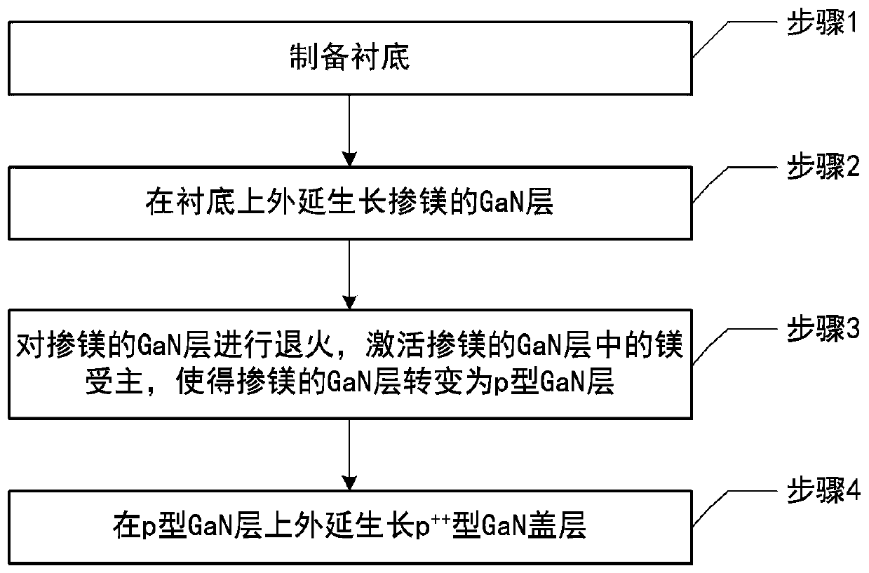
[0027] In order to make the purpose, technical solutions and advantages of the present disclosure clearer, the present disclosure will be further described in detail below in conjunction with specific embodiments and with reference to the accompanying drawings.

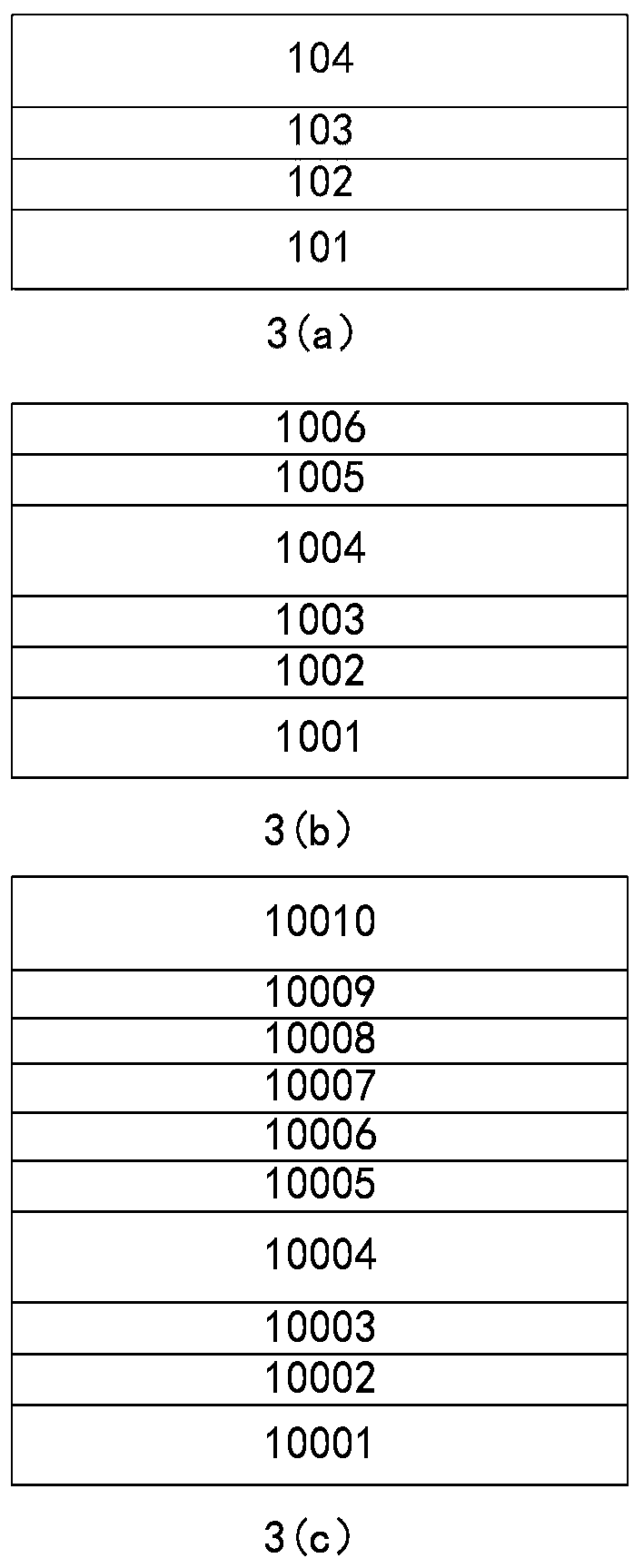
[0028] figure 1 A flowchart schematically shows a method for preparing a p-type GaN epitaxial wafer with high ohmic contact characteristics provided by an embodiment of the present disclosure. figure 2 A schematic structural diagram of a p-type GaN epitaxial wafer with high ohmic contact characteristics provided by an embodiment of the present disclosure is schematically shown. image 3 (a)-(c) respectively show the structural schematic diagrams of the substrates provided by the embodiments of the present disclosure. combine figure 2 and image 3 (a)-(c), yes figure 1 Described preparation method is described in detail, and this preparation method comprises:

[0029] Step 1: Prepare the substrate 10 .

[0030]...


PUM

PropertyMeasurementUnit
Thicknessaaaaaaaaaa
Thicknessaaaaaaaaaa

Abstract

The present invention provides a p-type GaN epitaxial wafer with high ohmic contact features and a preparation method thereof. The preparation method comprises the steps of: the step 1: preparing a substrate (10); the step 2: performing epitaxial growth of an Mg-doped GaN layer on the substrate (10); the step 3: performing annealing for the Mg-doped GaN layer to activate a magnesium acceptor in the Mg-doped GaN layer to convert the Mg-doped GaN layer to a p-type GaN epitaxial layer (11); and the step (4): performing epitaxial growth of a p++-type GaN cover layer (12) on the p-type GaN epitaxial layer (11). The heavily-doped p++-type GaN cover layer is grown on the p-type GaN layer, and the heavily-doped p++-type GaN cover layer does not perform high-temperature annealing to improve the quality of the ohmic contact layer of the epitaxial wafer and reduce the specific contact resistance rate of the contact of the p-type material and the metal.

Description

technical field [0001] The present disclosure relates to the technical field of semiconductor devices, in particular to a p-type GaN epitaxial wafer with high ohmic contact characteristics and a preparation method thereof. Background technique [0002] GaN-based materials are also known as Group III nitride materials (including InN, GaN, AlN, InGaN, AlGaN, etc., and their forbidden band width ranges from 0.7-6.2eV), and their spectra cover the near-infrared to deep ultraviolet bands. The third-generation semiconductor after Si and GaAs has important application value in the field of optoelectronics. In the 1990s, with the development of the two-step growth method and the p-type annealing activation method, GaN-based materials and devices have received extensive attention. At present, GaN-based lasers have been successfully applied to laser lighting, laser projection, laser TV, industrial processing and other fields. However, compared with GaAs, InP and other materials, GaN-...

Claims


Application Information

Patent Timeline
IPC IPC(8): H01L21/324H01L33/00H01L33/02H01S5/30
Inventor 杨静赵德刚朱建军陈平刘宗顺梁锋
Owner INST OF SEMICONDUCTORS - CHINESE ACAD OF SCI
Why Eureka
Try Eureka