Highly doped III-nitride semiconductors

a technology of iii-nitride and high mole fraction, which is applied in the direction of semiconductor devices, basic electric elements, electrical apparatus, etc., can solve the problems of poor electrical conductivity, and achieve the effect of reducing electrical resistance and high wall-plug efficiency

Inactive Publication Date: 2005-08-18
CORNELL RES FOUNDATION INC
View PDF20 Cites 7 Cited by
  • Summary
  • Abstract
  • Description
  • Claims
  • Application Information

AI Technical Summary

Benefits of technology

[0006] Highly doped, high Al mole fraction AlGaN provides reduced electrical resistance. The high levels of doping at high Al mole fraction provide application of n-type bulk, and n / p tunnel injection to short wavelength UV emitters with very high wall-plug efficiency.
[0007] Injection of holes into AlGaN through n+ / p+ tunnel junctions is used to replace thick p-AlGaN with n-AlGaN as a contact to multiple quantum well (MQW) emitters. High doping concentration provided by the current invention reduces AlGaN electrical resistance, and reduces the already small parasitic voltage drop and series resistance introduced by the tunnel junction. In one embodiment, n-GaN beyond 3×1020 cm−3, and n-Al0.65Ga0.35N beyond 1×1020 cm−3 electron concentrations are obtained.

Problems solved by technology

Difficulties in conventional approaches to UV emitter fabrication for short wavelengths are predominantly based on poor electrical conductivity in high Al mole fraction AlGaN, and high resistance contacts to these materials.

Method used


Image

  • Highly doped III-nitride semiconductors
  • Highly doped III-nitride semiconductors
  • Highly doped III-nitride semiconductors

Examples


Embodiment Construction

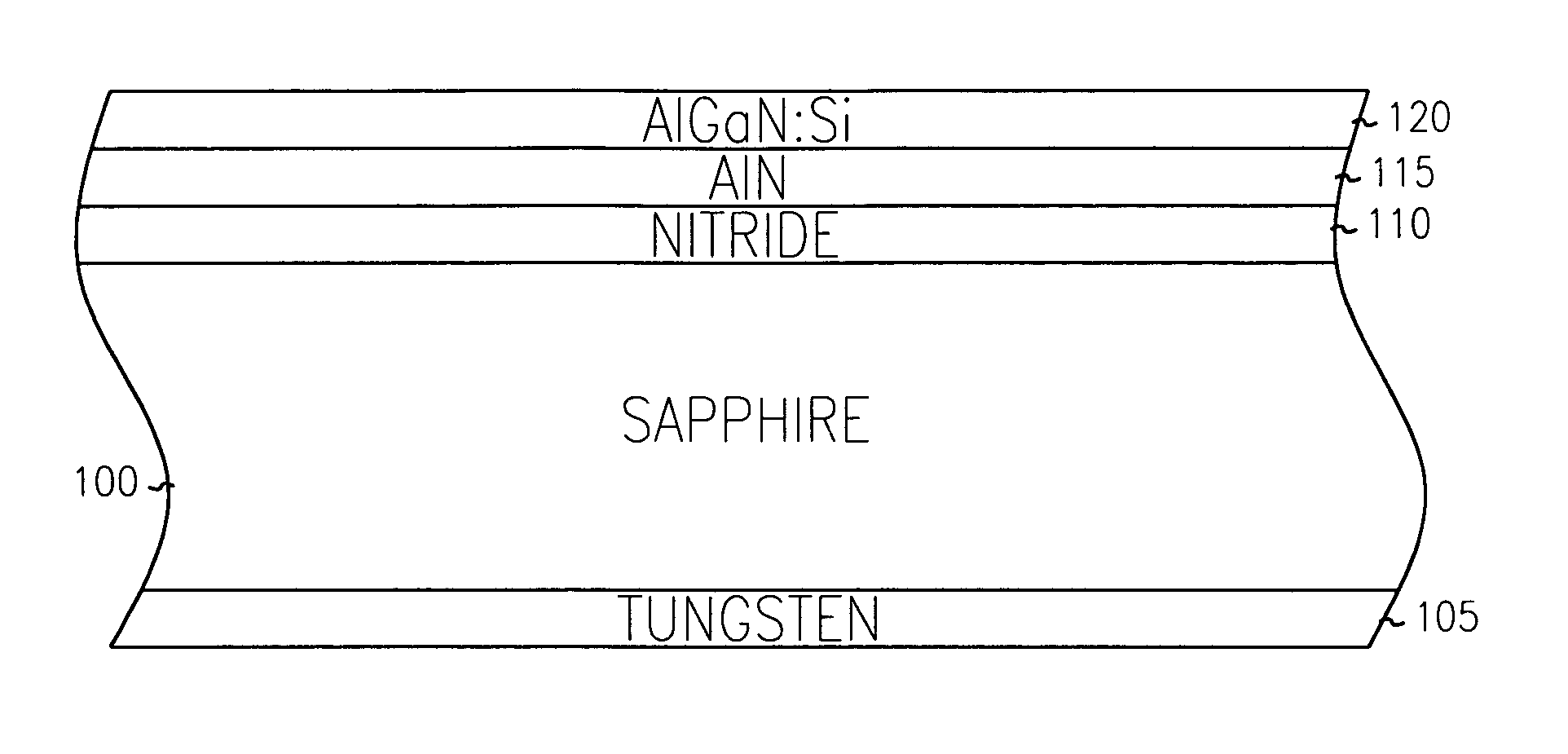
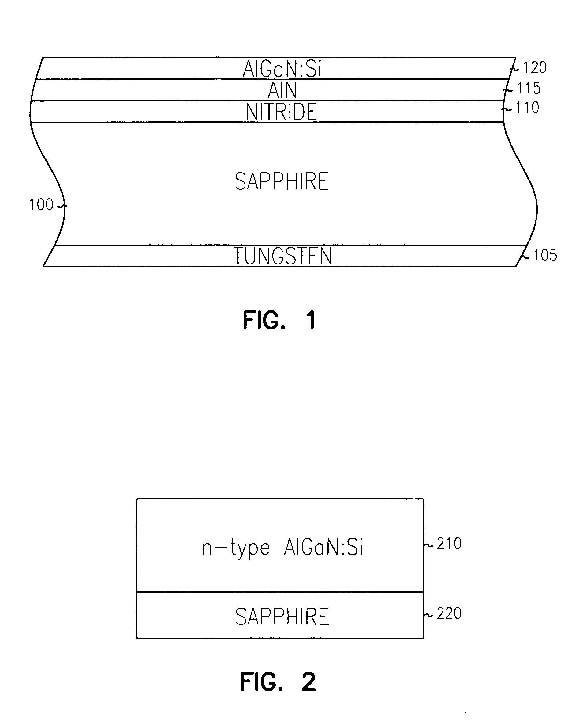
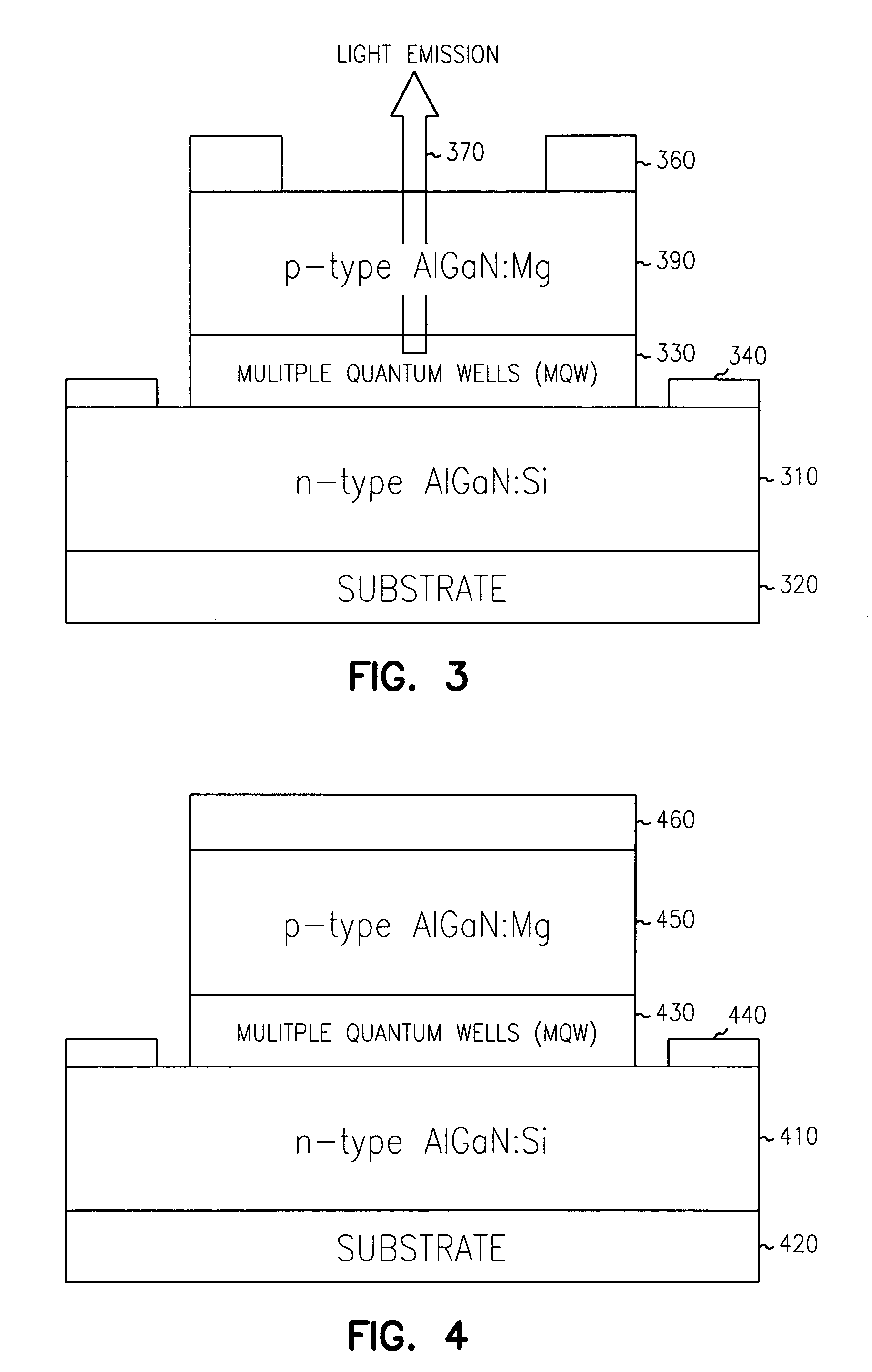
[0023] In the following description, reference is made to the accompanying drawings, which form a part hereof, and in which is shown by way of illustration specific embodiments in which the invention may be practiced. These embodiments are described in sufficient detail to enable those skilled in the art to practice the invention, and it is to be understood that other embodiments may be utilized and that structural, logical and electrical changes may be made without departing from the scope of the present invention. Ranges of values have been given for various parameters and expressed as typical, minimum and maximum for various embodiments. These are approximate values and should not be taken as absolutes. Further, potentially large variations in parameter values may occur for alternative embodiments without departing from the invention as claimed. The following description is, therefore, not to be taken in a limited sense, and the scope of the present invention is defined by the ap...


PUM


Abstract

A method of forming a highly doped layer of AlGaN, is practiced by first removing contaminants from a MBE machine. Wafers are then outgassed in the machine at very low pressures. A nitride is then formed on the wafer and an AlN layer is grown. The highly doped GaAlN layer is then formed having electron densities beyond 1×1020 cm−3 at Al mole fractions up to 65% are obtained. These levels of doping application of n-type bulk, and n / p tunnel injection to short wavelength UV emitters. Some applications include light emitting diodes having wavelengths between approximately 254 and 290 nm for use in fluorescent light bulbs, hazardous materials detection, water purification and other decontamination environments. Lasers formed using the highly doped layers are useful in high-density storage applications or telecommunications applications. In yet a further embodiment, a transistor is formed utilizing the highly doped layer as a channel.

Description

RELATED APPLICATION [0001] This application is a divisional of U.S. patent application Ser. No. 10 / 140,774, filed May 7, 2002, which claims the benefit of priority to U.S. Provisional Patent Application Ser. No. 60 / 364,499, filed Mar. 15, 2002, the entirety of which is incorporated herein by reference.GOVERNMENT FUNDING [0002] The invention described herein was made with U.S. Government support under Grant Number 0123453 awarded by the National Science Foundation. The United States Government has certain rights in the invention.FIELD OF THE INVENTION [0003] The present invention relates to degenerate doping of high mole fraction Nitrides, and in particular to increasing the conductivity of the AlGaN by high density doping for applications including light emitting diodes, lasers, transistors, light detectors, photovoltaic cells and thermocouple. BACKGROUND OF THE INVENTION [0004] UV emitters are formed using multiple quantum wells combined with electrical contacts to the wells. Such ...

Claims


Application Information

Patent Timeline
Patent Type & Authority Applications(United States)
IPC IPC(8): H01L21/203H01L29/15H01L29/20H01L29/778H01L33/32
CPCH01L21/0237H01L21/0242H01L21/02458H01L21/02507H01L21/0254H01L21/02576H01L33/325H01L21/02631H01L29/155H01L29/2003H01L29/7787H01L33/32H01L21/02579Y10S438/905
Inventor SCHAFF, WILLIAM J.HWANG, JEONGHYUN
Owner CORNELL RES FOUNDATION INC
Why Eureka
Try Eureka