OLED light-emitting device and preparation method thereof

A light-emitting device and optical path technology, which is applied in semiconductor/solid-state device manufacturing, electric solid-state devices, semiconductor devices, etc. Problems such as the difficulty of performance adjustment, to achieve the effect of improved color shift, low driving voltage, and reduced adjustment difficulty

Inactive Publication Date: 2014-11-19
EVERDISPLAY OPTRONICS (SHANGHAI) CO LTD
View PDF5 Cites 7 Cited by
  • Summary
  • Abstract
  • Description
  • Claims
  • Application Information

AI Technical Summary

Problems solved by technology

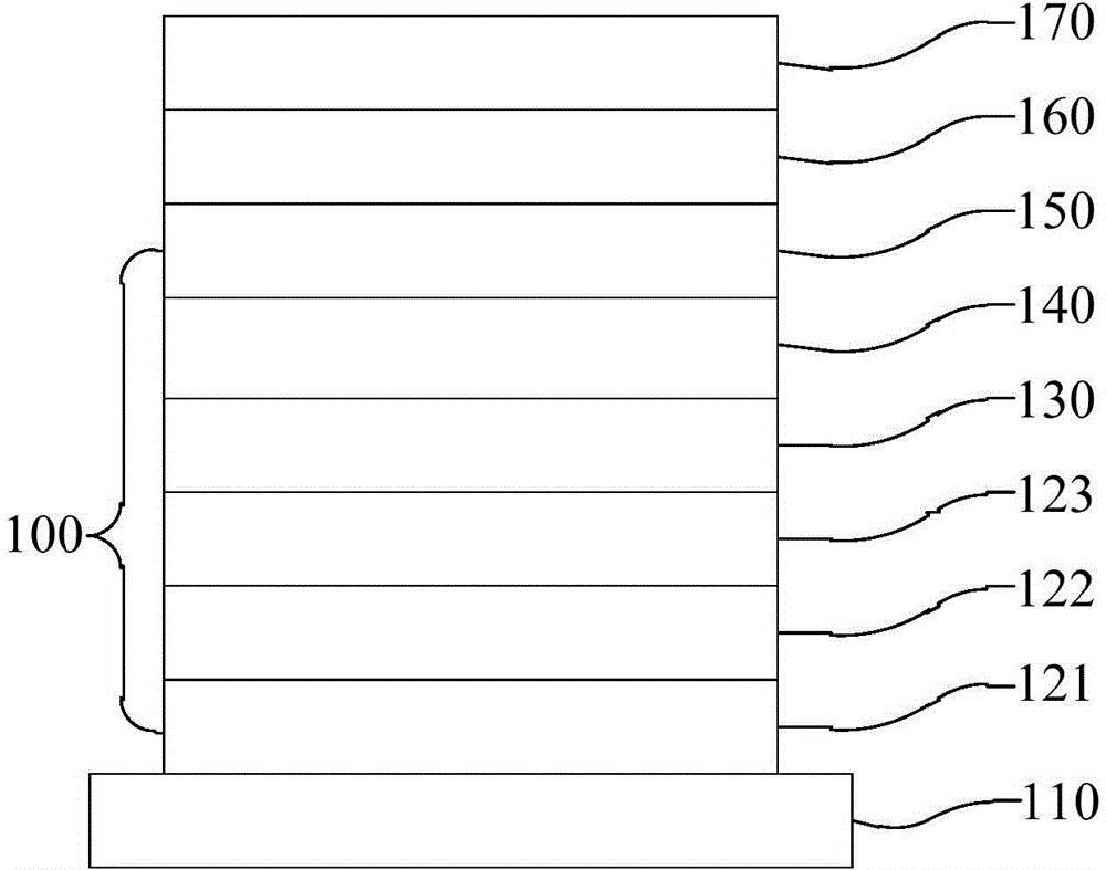
For example, the anode substrate 110, the organic functional layer 100, and the cathode layer 160 serve as both the electro-optical conversion part and the optical adjustment part. In this way, since the carrier mobility of the organic material is very low, if the total thickness of the organic functional layer changes, the OLED The driving voltage of the light-emitting device will also change accordingly, resulting in a change in the electrical properties of the device, which will increase the difficulty of adjusting the performance of the device; moreover, if the thickness of one or several layers in the organic functional layer is adjusted, it may cause The number of holes and electron carriers in the OLED light-emitting device becomes unbalanced, resulting in a decrease in the electro-optical conversion efficiency of the device

Method used


Image

  • OLED light-emitting device and preparation method thereof
  • OLED light-emitting device and preparation method thereof
  • OLED light-emitting device and preparation method thereof

Examples


specific Embodiment approach

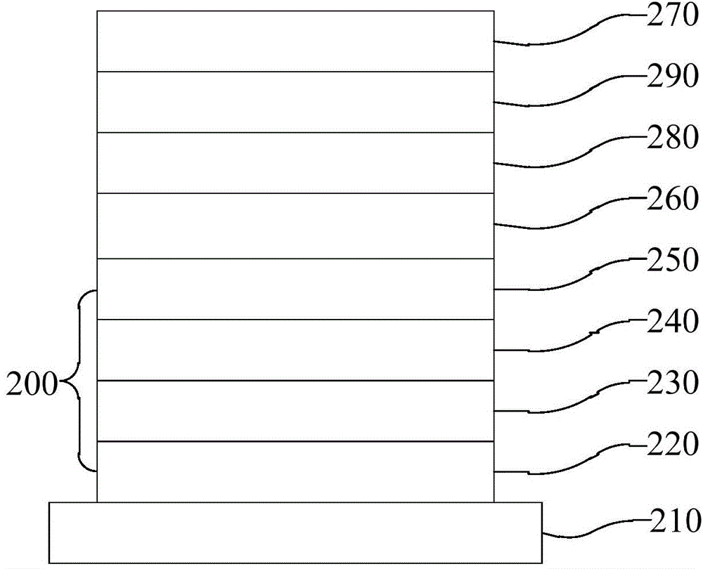
[0064]Example embodiments will now be described more fully with reference to the accompanying drawings. Example embodiments may, however, be embodied in many forms and should not be construed as limited to the embodiments set forth herein; rather, these embodiments are provided so that this disclosure will be thorough and complete, and will fully convey the concept of example embodiments to those skilled in the art. In the drawings, the thickness of regions and layers are exaggerated for clarity. The same reference numerals in the drawings denote the same or similar structures, and thus their detailed descriptions will be omitted.

[0065] Furthermore, the described features, structures, or characteristics may be combined in any suitable manner in one or more embodiments. In the following description, numerous specific details are provided in order to give a thorough understanding of embodiments of the present disclosure. However, one skilled in the art will appreciate that...


PUM


Abstract

The invention provides an OLED light-emitting device and a preparation method thereof. The OLED light-emitting device comprises a first electrode; an organic function layer formed on the first electrode; a second electrode formed on the organic function layer; an optical distance adjustment layer formed on the second electrode and used for adjusting the optical length of the OLED light-emitting device; and a semi-reflective semi-permeable layer formed on the optical distance adjustment layer and used for adjusting phase difference of the light emitted out from the optical distance adjustment layer when the light is reflecting. According to the OLED light-emitting device and the preparation method thereof, the adjustment difficulty of the device can be reduced, the production qualified rate is improved, and the cost is reduced. Besides, the thickness of the electro-optical conversion part of the device is far smaller than that of the structure in the prior art, so that drive voltage of the whole device gets smaller, electro-optical conversion efficiency of the device is improved at the meanwhile power consumption is reduced, and the service life of the device is increased. Besides, through the OLED light-emitting device, colour difference is also improved.

Description

technical field [0001] The present disclosure relates to the field of display technology, in particular to an OLED light-emitting device and a preparation method thereof. Background technique [0002] Compared with the liquid crystal display panel in the traditional technology, the OLED (Organic Light Emitting Diode, Organic Light Emitting Diode) display device has the characteristics of faster response speed, better color purity and brightness, higher contrast ratio, and wider viewing angle. Therefore, it has gradually received more and more attention from display technology developers. In the prior art, in order to improve the color purity and light intensity of OLED display devices and obtain a better color coordinate value, OLED light-emitting devices with a top-emission structure are usually used to facilitate the realization by adjusting the microcavity structure. Adjustment of the glow effect. [0003] Such as figure 1 It is a schematic structural diagram of a comm...

Claims


Application Information

Patent Timeline
Patent Type & Authority Applications(China)
IPC IPC(8): H01L51/52H01L51/56
CPCH10K50/852H10K50/85H10K50/856
Inventor 何志江黄初旺祝文秀张琨
Owner EVERDISPLAY OPTRONICS (SHANGHAI) CO LTD
Why Eureka
Try Eureka