Organic Light-Emitting Display Device

a display device and organic technology, applied in the field of organic light-emitting display devices, can solve the problems of low transmittance of transparent display devices, distorted image may be transmitted to users, etc., and achieve the effect of reducing voltage drop and improving transmittance in transmitting regions

Active Publication Date: 2011-08-25
SAMSUNG DISPLAY CO LTD
View PDF30 Cites 80 Cited by
  • Summary
  • Abstract
  • Description
  • Claims
  • Application Information

AI Technical Summary

Benefits of technology

[0011]The present invention relates to an organic light-emitting display device which can be transparent by improving a transmittance in transmitting regions, and which can reduce a voltage drop in an opposite electrode.

Problems solved by technology

However, the transmittances of the organic light-emitting diodes, the thin film transistors and the wires are not so high, and spaces between the organic light-emitting diodes, the thin film transistor and the wires are very small, and thus the transmittance of the transparent display device is not high.
Also, a distorted image may be transmitted to the user due to the patterns of the organic light-emitting diodes, the thin film transistors and the wires.

Method used


Image

  • Organic Light-Emitting Display Device
  • Organic Light-Emitting Display Device
  • Organic Light-Emitting Display Device

Examples


Embodiment Construction

[0055]The present invention will now be described more fully with reference to the accompanying drawings in which exemplary embodiments of the invention are shown.

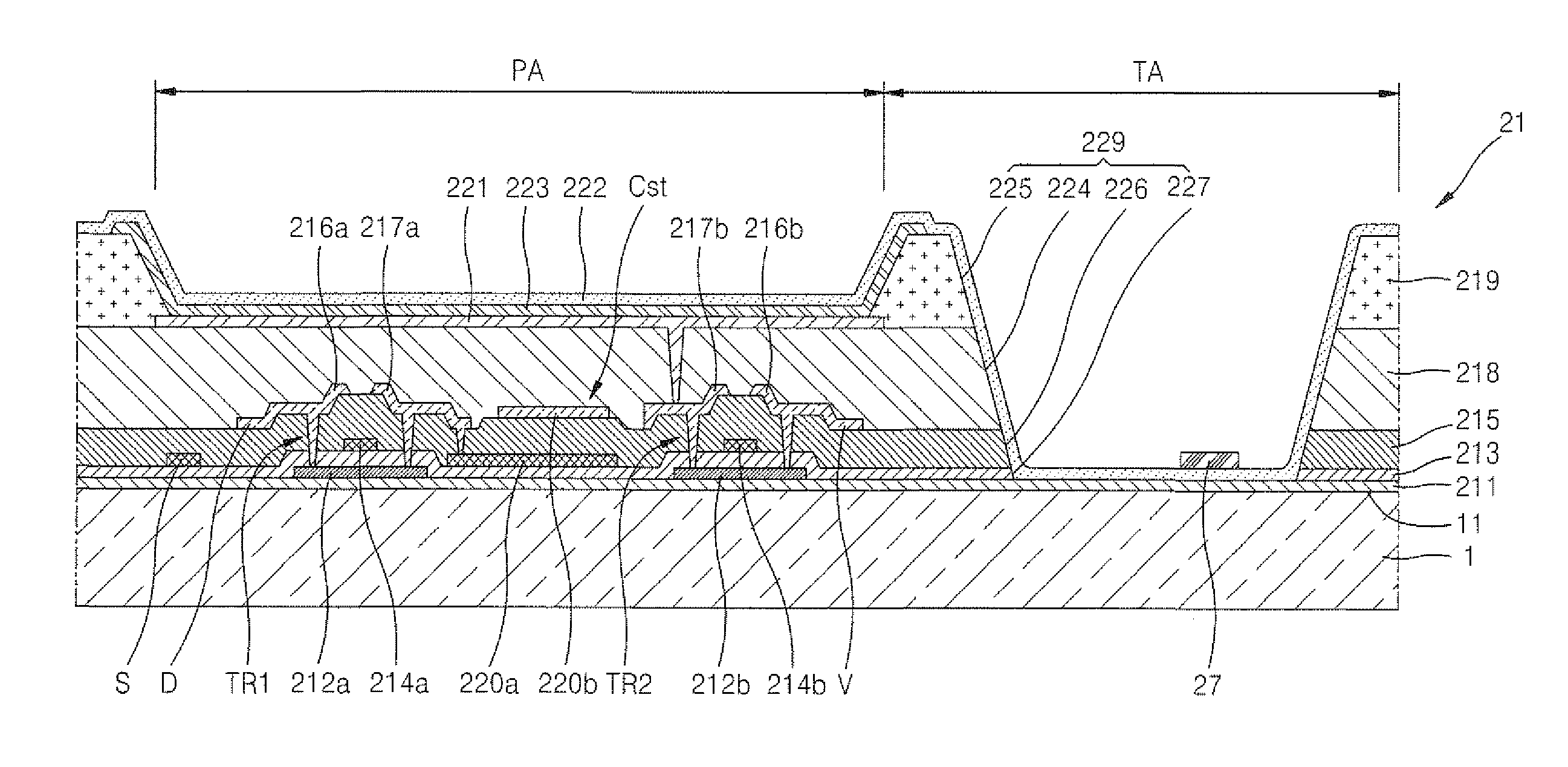
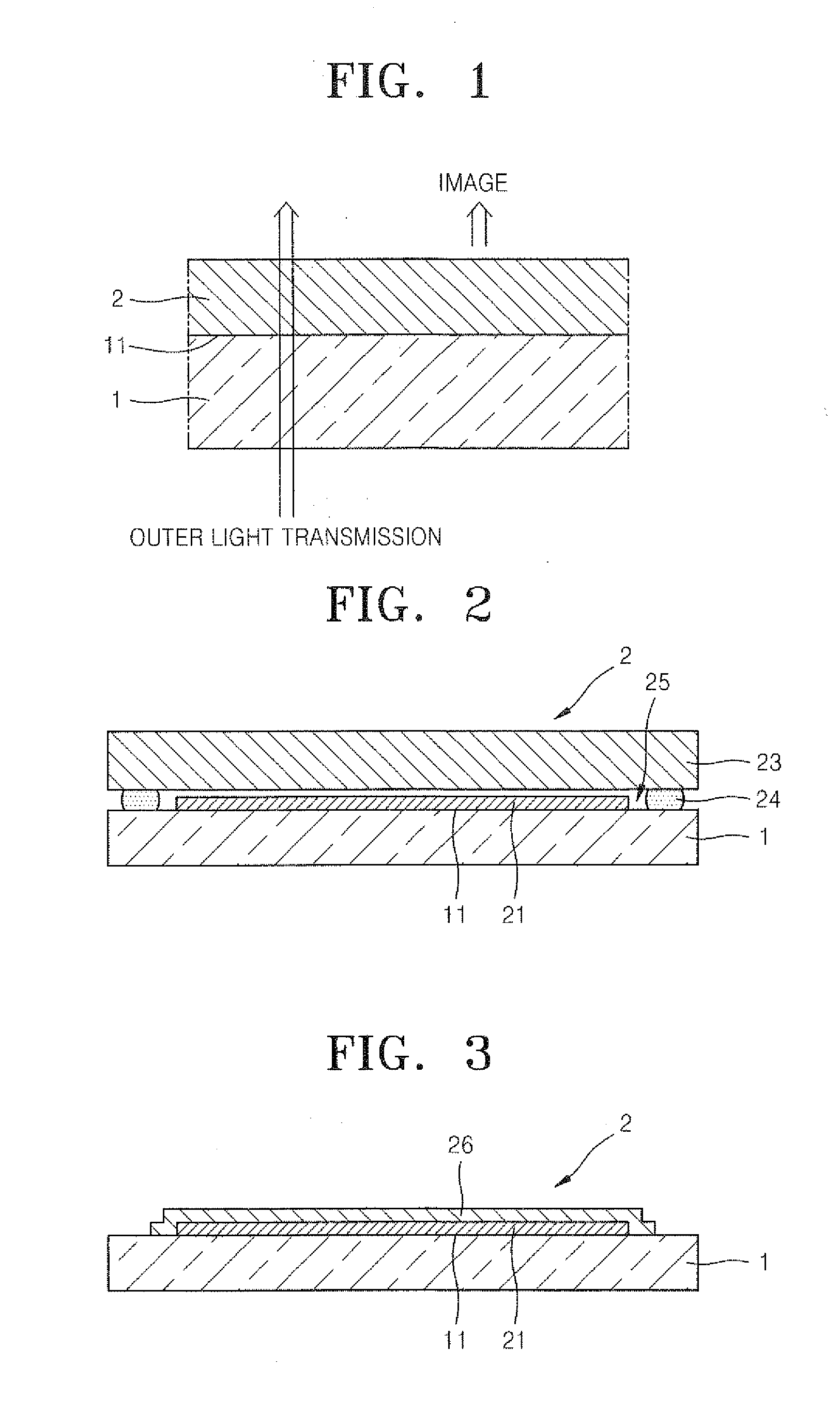
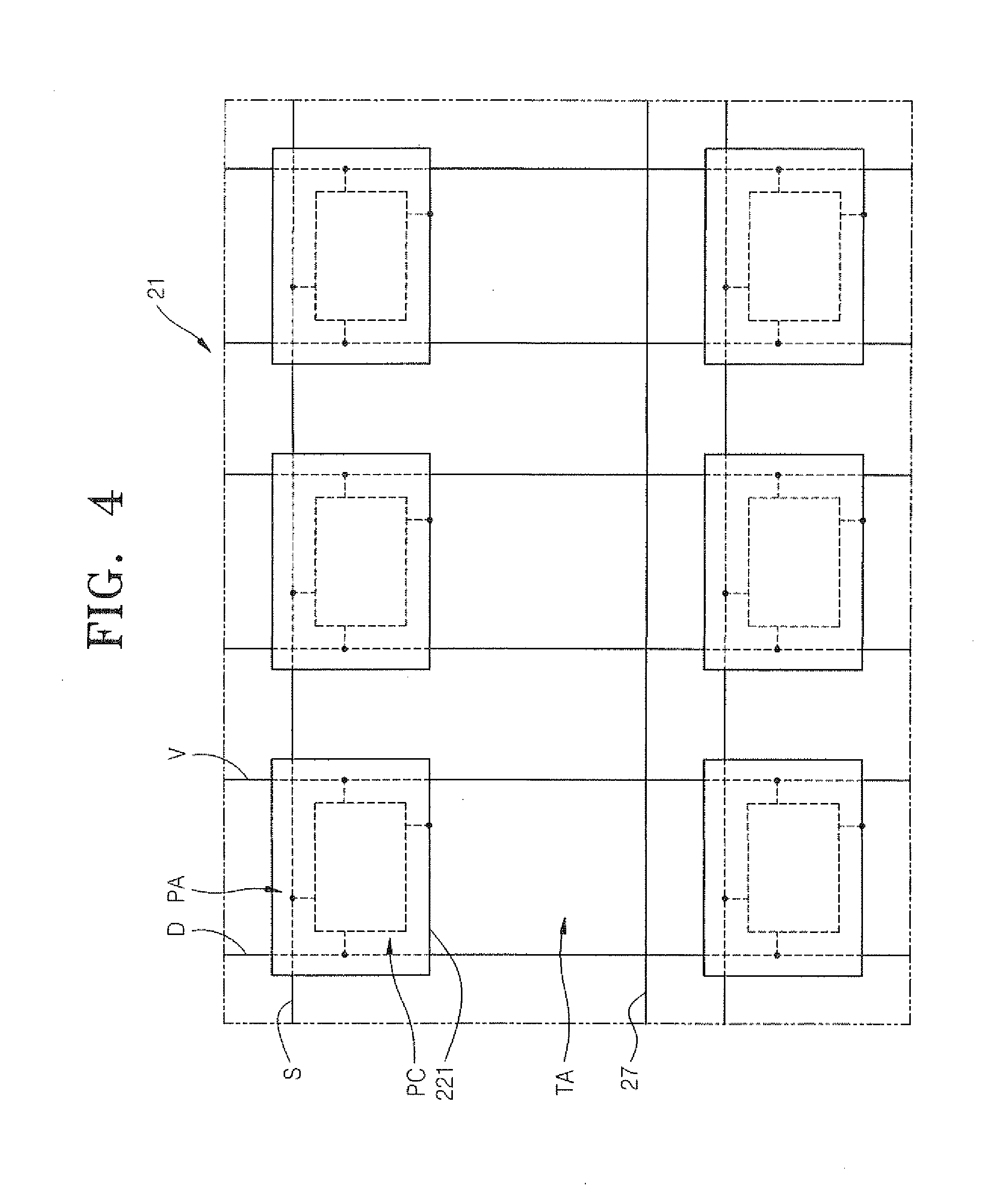
[0056]FIG. 1 is a cross-sectional view of an organic light-emitting display device according to an embodiment of the present invention.

[0057]Referring to FIG. 1, the organic light-emitting display device according to the current embodiment of the present invention includes a display unit 2 formed on a first surface 11 of a substrate 1.

[0058]In the organic light-emitting display device, external light enters through the substrate 1 and the display unit 2.

[0059]As will be described later, the display unit 2 is formed so as to be able to transmit external light. That is, referring to FIG. 1, the display unit 2 is formed in such a way that a user positioned on a side where an image is displayed can observe an object outside the substrate 1.

[0060]FIG. 2 is a cross-sectional view of the organic light-emitting display device of F...


PUM


Abstract

An organic light-emitting display device which is transparent by improving a transmittance in transmitting regions and which reduces a voltage drop in an opposite electrode comprises: a substrate having a transmitting region and pixel regions separated from each other by the transmitting region; thin film transistors positioned on the substrate and disposed in the pixel regions, respectively; a passivation layer covering the thin film transistors, formed in the transmitting region and the pixel regions, and having a first opening formed in a location corresponding to at least a portion of the transmitting region; pixel electrodes formed on the passivation layer so as to be electrically connected to the thin film transistors, respectively, located in the pixel regions, and disposed so as to overlap and cover the thin film transistors, respectively; an opposite electrode facing the pixel electrodes, formed so as to be able to transmit light, and located in the transmitting region and the pixel regions; an organic emission layer interposed between the pixel electrodes and the opposite electrode so as to emit light; and a conduction unit formed of a conductive material, disposed so as to overlap with the first opening, and contacting the opposite electrode.

Description

CLAIM OF PRIORITY[0001]This application makes reference to, incorporates the same herein, and claims all benefits accruing under 35 U.S.C. §119 from an application earlier filed in the Korean Intellectual Property Office on the 19 Feb. 2010 and there duly assigned Serial No. 10-2010-00015241.BACKGROUND OF THE INVENTION[0002]1. Field of the Invention[0003]The present invention relates to an organic light-emitting display device and, more particularly, to a transparent organic light-emitting display device.[0004]2. Description of the Related Art[0005]Applications of organic light-emitting display devices range from personal portable devices, such as MP3 players and mobile phones, to television sets due to their having superior characteristics such as wide viewing angles, high contrast ratios, short response times, and low amounts of power consumption.[0006]An organic light-emitting display device has self-light emitting characteristics, and the weight and thickness of the organic ligh...

Claims


Application Information

Patent Timeline
Patent Type & Authority Applications(United States)
IPC IPC(8): H01L51/52
CPCH01L51/5228H01L51/5234H01L27/3276H01L2251/5323H01L27/326H01L2251/5315H10K59/121H10K59/131H10K50/824H10K50/828H10K2102/3026H10K2102/3031H05B33/26
Inventor HA, JAE-HEUNGHWANG, KYU-HWANYOON, SEOK-GYUSONG, YOUNG-WOOLEE, JONG-HYUKCHOI, JUN-HOCHUNG, JIN-KOO
Owner SAMSUNG DISPLAY CO LTD
Why Eureka
Try Eureka