

Methods to Enhance Effective Work Function of Mid-Gap Metal by Incorporating Oxygen and Hydrogen at a Low Thermal Budget
a technology of oxygen and hydrogen and a low thermal budget, applied in the field of integrated circuits, can solve the problems of difficult to increase the fabrication cost and complexity of metal gates in pmos transistors without significantly increasing the work function of metal gates, and achieve the effect of increasing the effective work function
- Summary
- Abstract
- Description
- Claims
- Application Information
AI Technical Summary
Benefits of technology
Problems solved by technology
Method used
Image

Examples
first embodiment
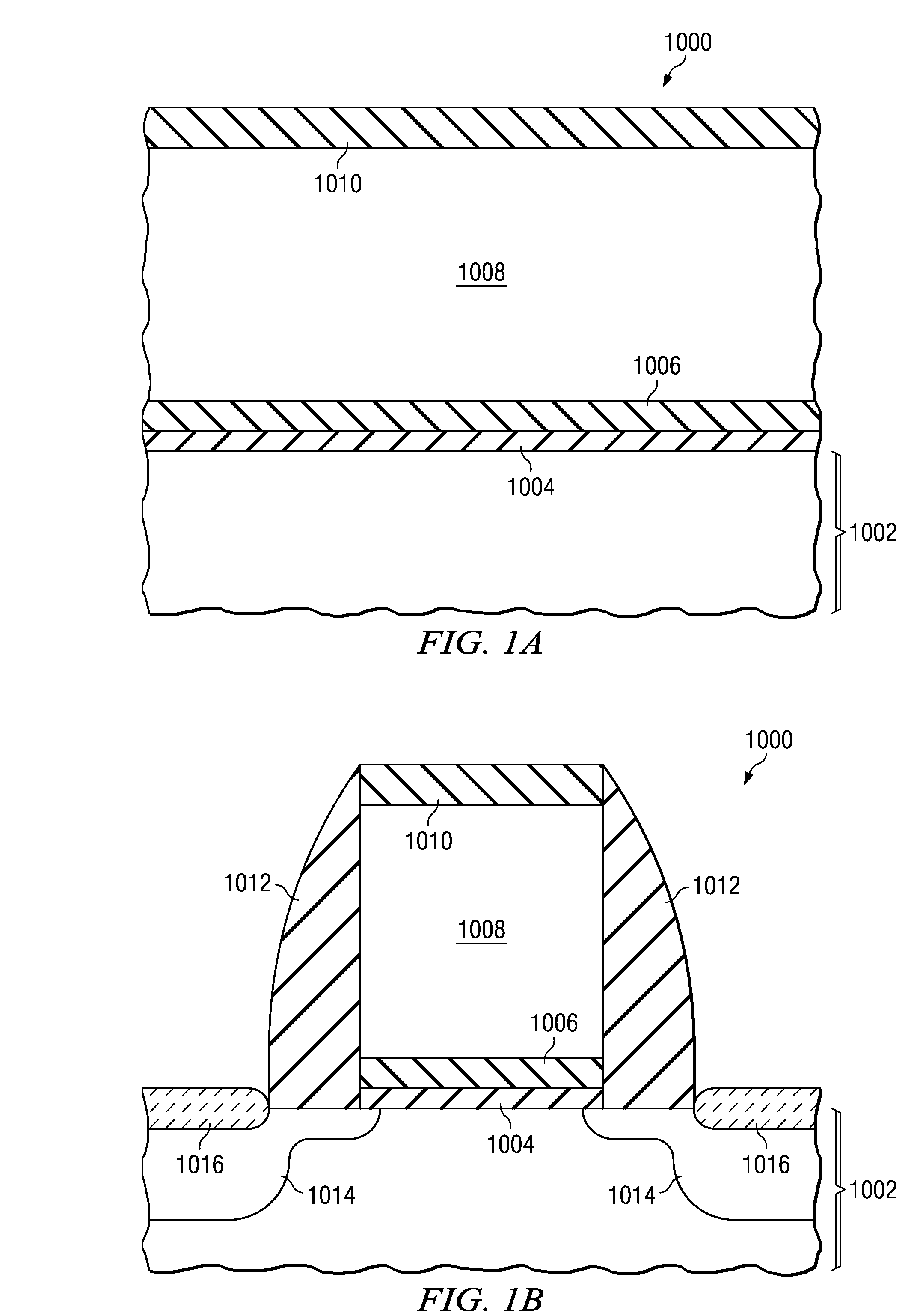
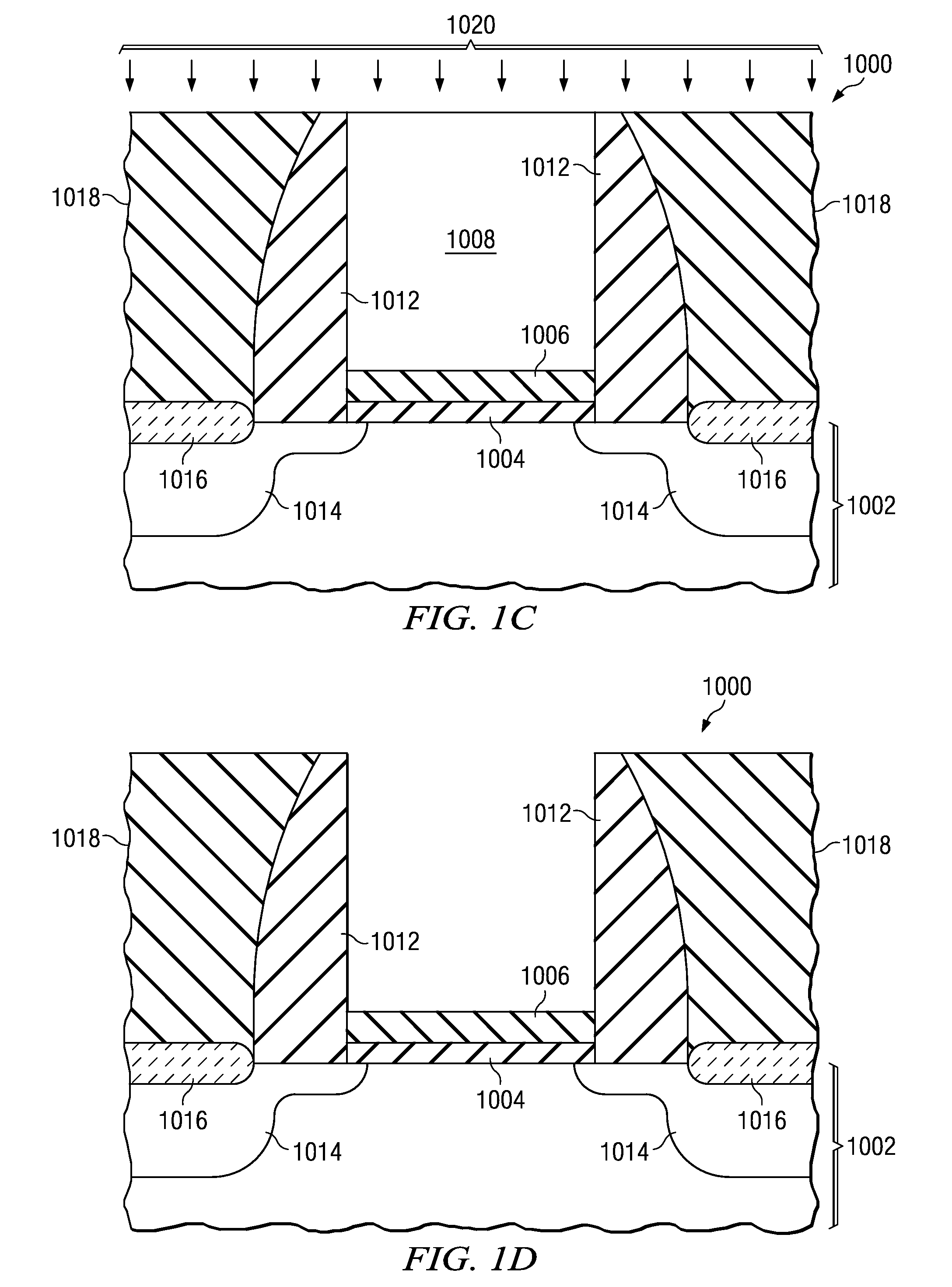
[0030]FIG. 2 is a cross-section of an integrated circuit containing a PMOS transistor formed according to the instant invention, depicted during a low temperature oxidation process to diffuse oxygen atoms into a PMOS gate work function metal layer. The integrated circuit 2000 is formed on a substrate 2002 as described in reference to FIG. 1A. A PMOS gate structure including a PMOS gate dielectric layer 2004, a PMOS gate work function metal layer 2006 and PMOS gate sidewall spacers 2008 is formed on a top surface of the substrate 2002 as described in reference to FIG. 1A through FIG. 1D. PSD regions 2010 are formed in the substrate 2002 adjacent to the PMOS gate dielectric layer 2004, and PSD silicide layers 2012 are formed on a top surface of the PSD regions 2010, as described in reference to FIG. 1B. An oxide fill layer 2014 is formed on a top surface of the integrated circuit 2000 in contact with the PMOS gate sidewall spacers 2008, as described in reference to FIG. 1C. A dummy ga...
second embodiment
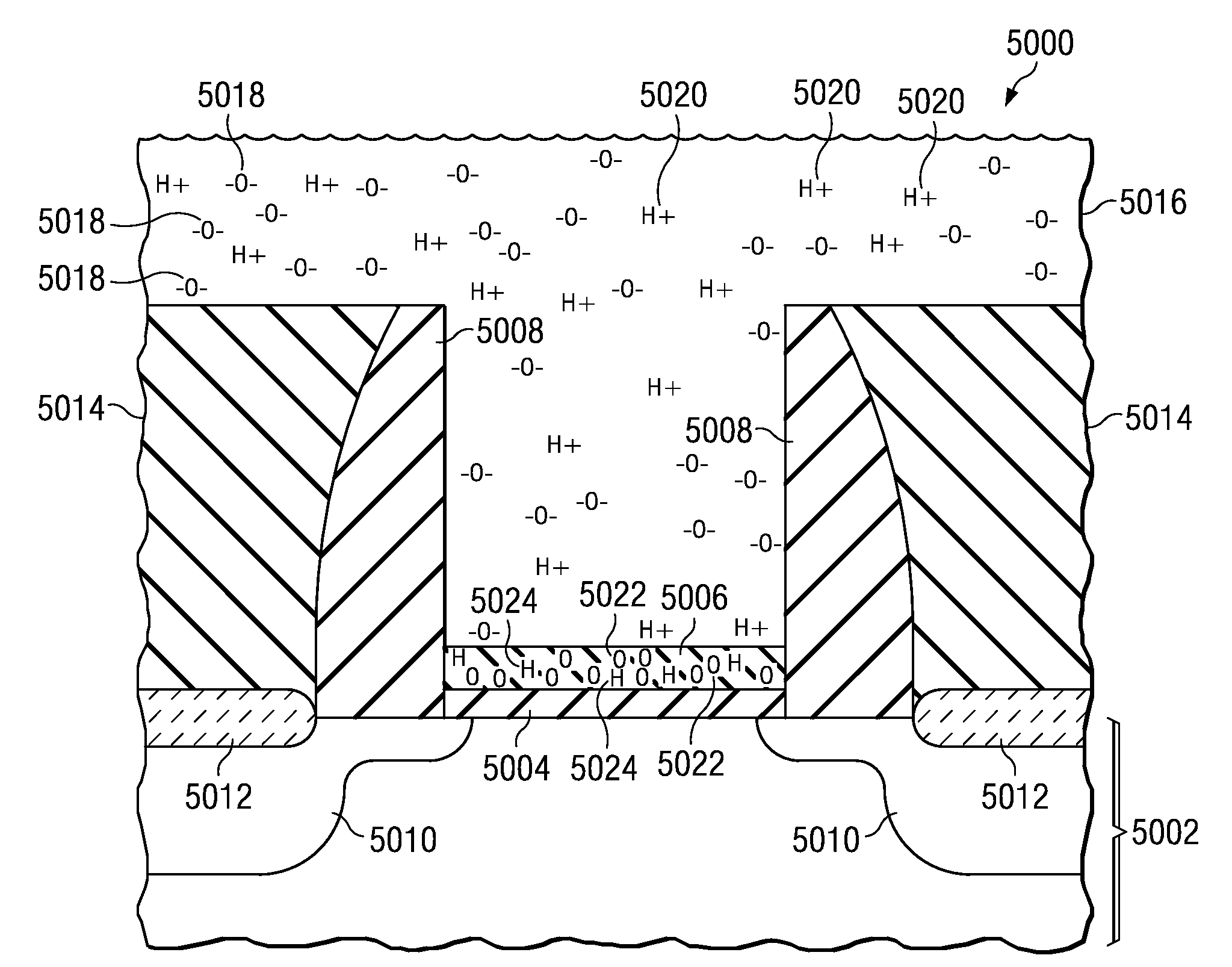
[0034]FIG. 3 is a cross-section of an integrated circuit containing a PMOS transistor formed according to the instant invention, depicted during a low temperature oxidation process to diffuse oxygen atoms into a PMOS gate work function metal layer. The integrated circuit 3000 is formed on a substrate 3002 as described in reference to FIG. 1A. A PMOS gate structure including a PMOS gate dielectric layer 3004, a PMOS gate work function metal layer 3006 and PMOS gate sidewall spacers 3008 is formed on a top surface of the substrate 3002 as described in reference to FIG. 1A through FIG. 1D. PSD regions 3010 are formed in the substrate 3002 adjacent to the PMOS gate dielectric layer 3004, and PSD silicide layers 3012 are formed on a top surface of the PSD regions 3010, as described in reference to FIG. 1B. An oxide fill layer 3014 is formed on a top surface of the integrated circuit 3000 in contact with the PMOS gate sidewall spacers 3008, as described in reference to FIG. 1C. A dummy ga...
third embodiment
[0038]FIG. 4A and FIG. 4B are cross-sections of an integrated circuit containing a PMOS transistor formed according to the instant invention, depicted during a low temperature oxidation process to diffuse oxygen atoms into a PMOS gate work function metal layer. Referring to FIG. 4A, the integrated circuit 4000 is formed on a substrate 4002 as described in reference to FIG. 1A. A PMOS gate structure including a PMOS gate dielectric layer 4004, a PMOS gate work function metal layer 4006 and PMOS gate sidewall spacers 4008 is formed on a top surface of the substrate 4002 as described in reference to FIG. 1A through FIG. 1D. PSD regions 4010 are formed in the substrate 4002 adjacent to the PMOS gate dielectric layer 4004, and PSD silicide layers 4012 are formed on a top surface of the PSD regions 4010, as described in reference to FIG. 1B. An oxide fill layer 4014 is formed on a top surface of the integrated circuit 4000 in contact with the PMOS gate sidewall spacers 4008, as described ...
PUM
| Property | Measurement | Unit |
|---|---|---|
| work functions | aaaaa | aaaaa |
| work functions | aaaaa | aaaaa |
| work function | aaaaa | aaaaa |
Abstract
Description
Claims
Application Information