Method of manufacturing silicon single crystal

a manufacturing method and silicon single crystal technology, applied in the direction of polycrystalline material growth, crystal growth process, polycrystalline material growth, etc., can solve the problems of bubble formation, pinhole defect, and still a possibility of new occurrence of bubbles, so as to suppress the formation of pinholes

Inactive Publication Date: 2011-09-08
GLOBALWAFERS JAPAN
View PDF5 Cites 22 Cited by
  • Summary
  • Abstract
  • Description
  • Claims
  • Application Information

AI Technical Summary

Benefits of technology

[0008]The invention has been made to solve the above-mentioned technical problems, and an object thereof is to provide a method of manufacturing a silicon single crystal which can more greatly suppress the pinhole formation in the silicon single crystal.
[0012]According to the present invention, the method of manufacturing the silicon single crystal which can more greatly suppress the pinhole formation in the silicon single crystal is provided.

Problems solved by technology

In recent years, when pulling up a silicon single crystal, there is a problem that bubbles exist in silicon melt tend to be trapped within a silicon single crystal and a pinhole defect tends to occur.
However, according to the method disclosed in the patent document 1, although incidence of pinhole defects can be decreased by performing a melting process under a reduced pressure of 5 to 60 millibar, there is still a possibility of new occurrence of bubbles during the pulling up of the silicon single crystal.
Thus, it has limitation in suppression of the pinhole formation in the silicon single crystal.
However, in the case where the internal furnace pressure during the pulling up of the silicon single crystal is lower than the pressure during the melting process, there is still a possibility of new occurrence of bubbles in the silicon melt.
Thus, it has limitation in suppression of the pinhole formation in the silicon single crystal.

Method used


Image

  • Method of manufacturing silicon single crystal
  • Method of manufacturing silicon single crystal
  • Method of manufacturing silicon single crystal

Examples


examples

[0055]The present invention will be further described with reference to Examples, but the present invention is not limited thereto.

experiment 1

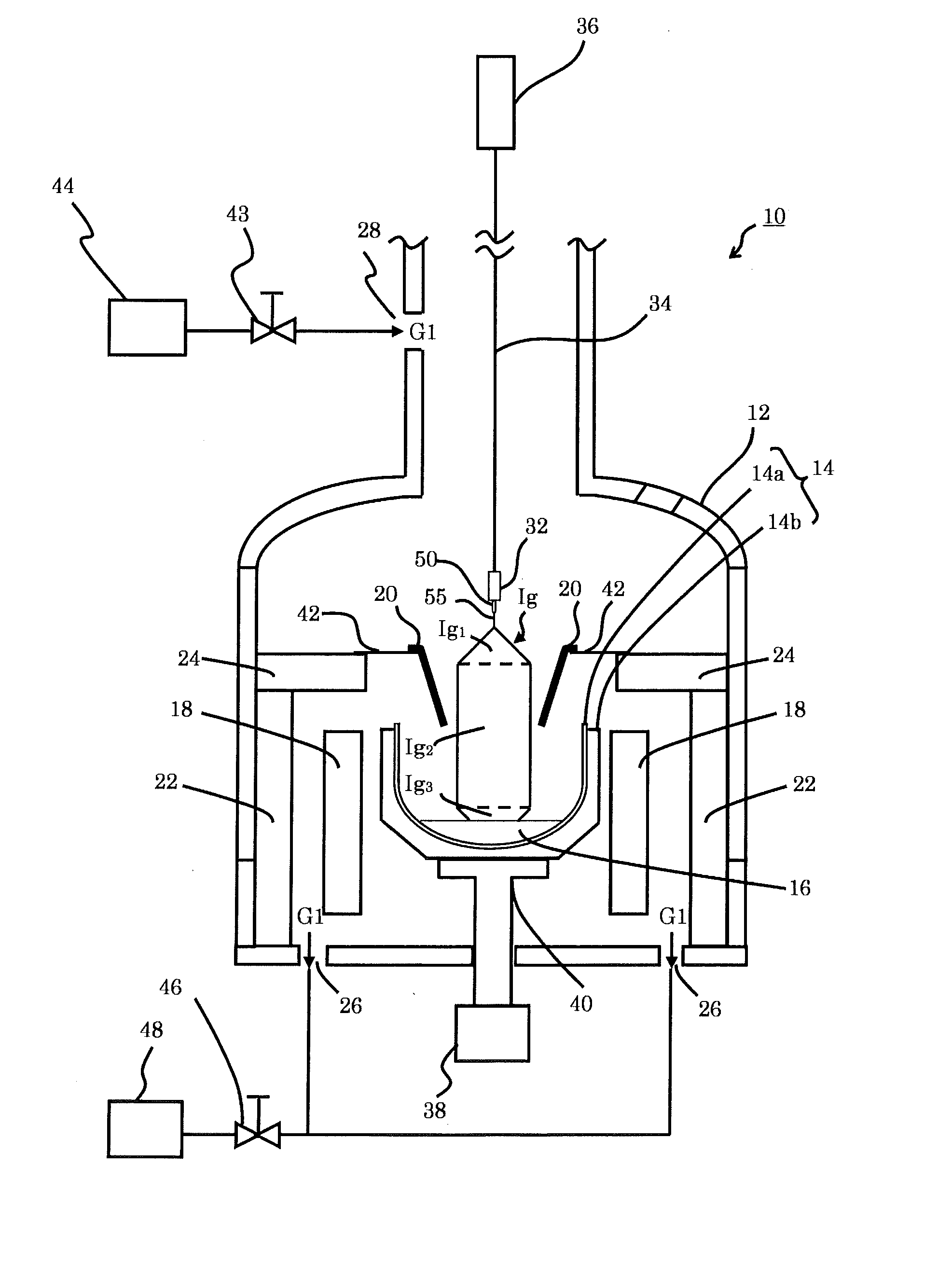
[0056]A P-type silicon single crystal Ig having a straight body Ig2 having a crystal orientation of and a diameter of 310 mm was manufactured from 300 kg of silicon material by using the silicon single crystal pulling up apparatus 10 shown in FIG. 1.

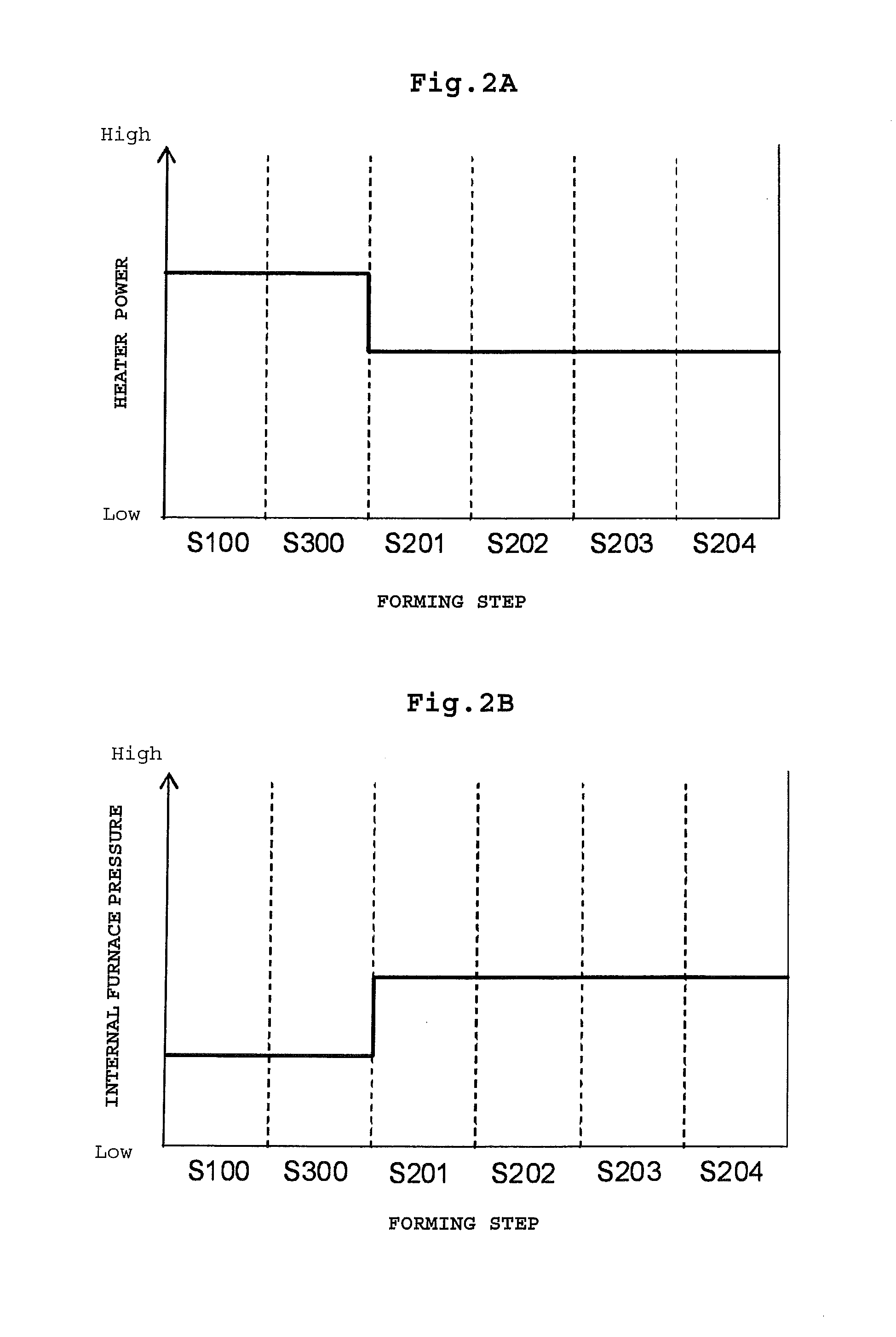
[0057]At this time, the heater power control and the internal furnace pressure control as shown in FIGS. 2A and 2B were carried out such that after the melting of the silicon material and before starting the pulling up of the silicon single crystal (step S300), the heater power was increased by 5% compared to that during the pulling up of the silicon single crystal and the silicon melt was held under various conditions by changing the internal furnace pressure and a period of time for maintaining the pressure level. The heater power level was then turned back and the internal furnace pressure was set at 80 Torr. Ten silicon single crystals were pulled up for each condition (Examples from 1 to 7, Comparative example 1).

[0058]In addition,...

experiment 2

[0063]A P-type silicon single crystal Ig having a straight body Ig2 having a crystal orientation of and a diameter of 310 mm was manufactured from 300 kg of the silicon material by using the silicon single crystal pulling up apparatus 10 shown in FIG. 1.

[0064]At this time, the heater power output control and the internal furnace pressure control as shown in FIGS. 2A and 2B were carried out such that after the melting of the silicon material and before starting the pulling up of the silicon single crystal (step S300), the heater power was increased by 5% compared to the heater power during the pulling up of the silicon single crystal and the silicon melt was held under various conditions by changing the internal furnace pressure and a period of time for maintaining the pressure level. The heater power level was then turned back and the internal furnace pressure was set at 40 Torr. Ten silicon single crystals were pulled up for each condition (Examples from 8 to 14, Comparative examp...


PUM

PropertyMeasurementUnit
pressureaaaaaaaaaa
pressureaaaaaaaaaa
pressureaaaaaaaaaa

Abstract

The present invention provides a method of manufacturing a silicon single crystal which can more greatly suppress a pinhole formation in the silicon single crystal, which is a method of manufacturing a silicon single crystal by the Czochralski method in which a silicon material to be silicon melt is melted in a furnace body and then a silicon single crystal is pulled up. After melting the silicon material and before the start of pulling up the silicon single crystal, a heater power is set to be higher than that during the step of pulling up the silicon single crystal, and an internal furnace pressure is set as 30 Torr or less, which is lower than that during the step of pulling up the silicon single crystal, the power and pressure being maintained for a predetermined time, and then the step of pulling up the silicon single crystal is carried out.

Description

BACKGROUND OF THE INVENTION[0001]1. Field of the Invention[0002]The present invention relates to a method of manufacturing a silicon single crystal using the Czochralski method (hereinafter referred to as the “CZ method”), and more particularly to a method of manufacturing a silicon single crystal which can suppress pinhole formation in the silicon single crystal.[0003]2. Description of the Related Art[0004]In recent years, when pulling up a silicon single crystal, there is a problem that bubbles exist in silicon melt tend to be trapped within a silicon single crystal and a pinhole defect tends to occur.[0005]For such a problem, for example, in Japanese Patent Application Laid-Open (kokai) No. 5-9097 (patent document 1), a method in which polysilicon material is melted at an internal furnace pressure of from 5 to 60 millibar and then a silicon single crystal is pulled up at an internal furnace pressure of at least 100 millibar is disclosed. In Japanese Patent Application Laid-Open (...

Claims


Application Information

Patent Timeline
Patent Type & Authority Applications(United States)
IPC IPC(8): C30B15/14
CPCC30B15/14C30B29/06
Inventor MINAMI, TOSHIRO
Owner GLOBALWAFERS JAPAN
Why Eureka
Try Eureka