Reflection Mode Package for Optical Devices Using Gallium and Nitrogen Containing Materials

a gallium and nitrogen-containing material, optical device technology, applied in the field of lighting, can solve the problems of achieving high intensity, conventional light bulbs routinely fail, and discharging more than 90% of thermal energy used by conventional light bulbs, and achieve the effect of improving efficiency and being easy to implemen

Inactive Publication Date: 2011-09-08
SORAA
View PDF100 Cites 65 Cited by
  • Summary
  • Abstract
  • Description
  • Claims
  • Application Information

AI Technical Summary

Benefits of technology

[0014]The present device and method provides for an improved lighting with improved efficiency. The method and resulting structure are easier to implement using conventional technologies. In a specific embodiment, a violet-emitting LED device is capable of emitting electromagnetic radiation at a wavelength range from about 380 nanometers to about 440 nanometers. In another embodiment, a blue-emitting LED device is capable of emitting electromagnetic radiation at a wavelength range from about 440 nanometers to about 490 nm. In other embodiments, a plurality of LED devices with a plurality of emission wavelengths are employed.

Problems solved by technology

Unfortunately, the conventional light bulb dissipates more than 90% of the energy used as thermal energy.
Additionally, the conventional light bulb routinely fails due to thermal expansion and contraction of the filament element.
Unfortunately, achieving high intensity, high-efficiency GaN-based green LEDs has been problematic.
The light emission efficiency of typical GaN-based LEDs drops off significantly at higher current densities, as are required for general illumination applications, a phenomenon known as “roll-over.” Additionally, packages incorporating LEDs also have limitations.
Such packages often have thermal inefficiencies.
Other limitations include poor yields, low efficiencies, and reliability issues.

Method used


Image

  • Reflection Mode Package for Optical Devices Using Gallium and Nitrogen Containing Materials
  • Reflection Mode Package for Optical Devices Using Gallium and Nitrogen Containing Materials
  • Reflection Mode Package for Optical Devices Using Gallium and Nitrogen Containing Materials

Examples


Embodiment Construction

[0019]Recent breakthroughs in GaN-based optoelectronics demonstrate the potential of devices fabricated on bulk GaN substrates, including polar, nonpolar and semipolar orientations. For nonpolar and semipolar orientations, lack of strong polarization induced electric fields that plague conventional devices on c-plane (i.e., polar) GaN leads to a greatly enhanced radiative recombination efficiency in the light emitting InGaN layers. Furthermore, the nature of the electronic band structure and the anisotropic in-plane strain leads to highly polarized light emission, which offers advantages in applications such as display backlighting.

[0020]Of particular importance to the field of lighting is the progress of light emitting diodes (LED) fabricated on nonpolar and semipolar GaN substrates. Such devices making use of InGaN light emitting layers have exhibited record output powers at extended operation wavelengths into the violet region (390-430 nm), the blue region (430-490 nm), the green...


PUM

PropertyMeasurementUnit
thicknessaaaaaaaaaa
reflectivityaaaaaaaaaa
thicknessaaaaaaaaaa

Abstract

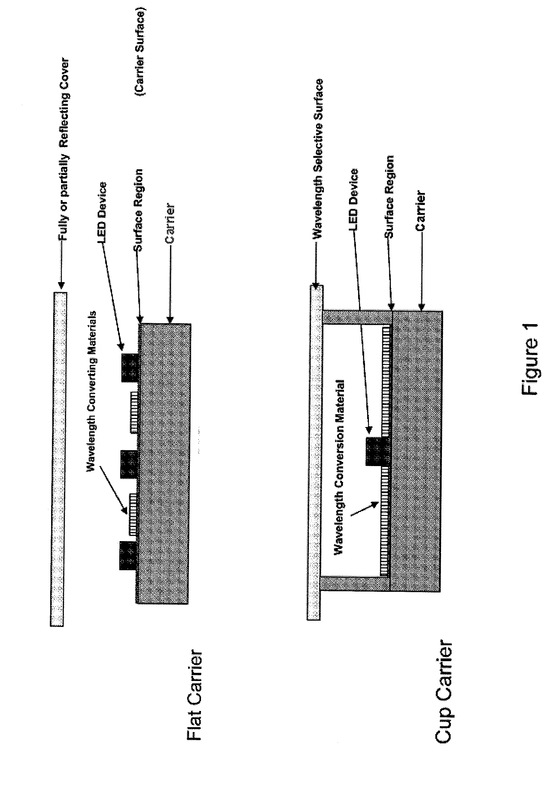
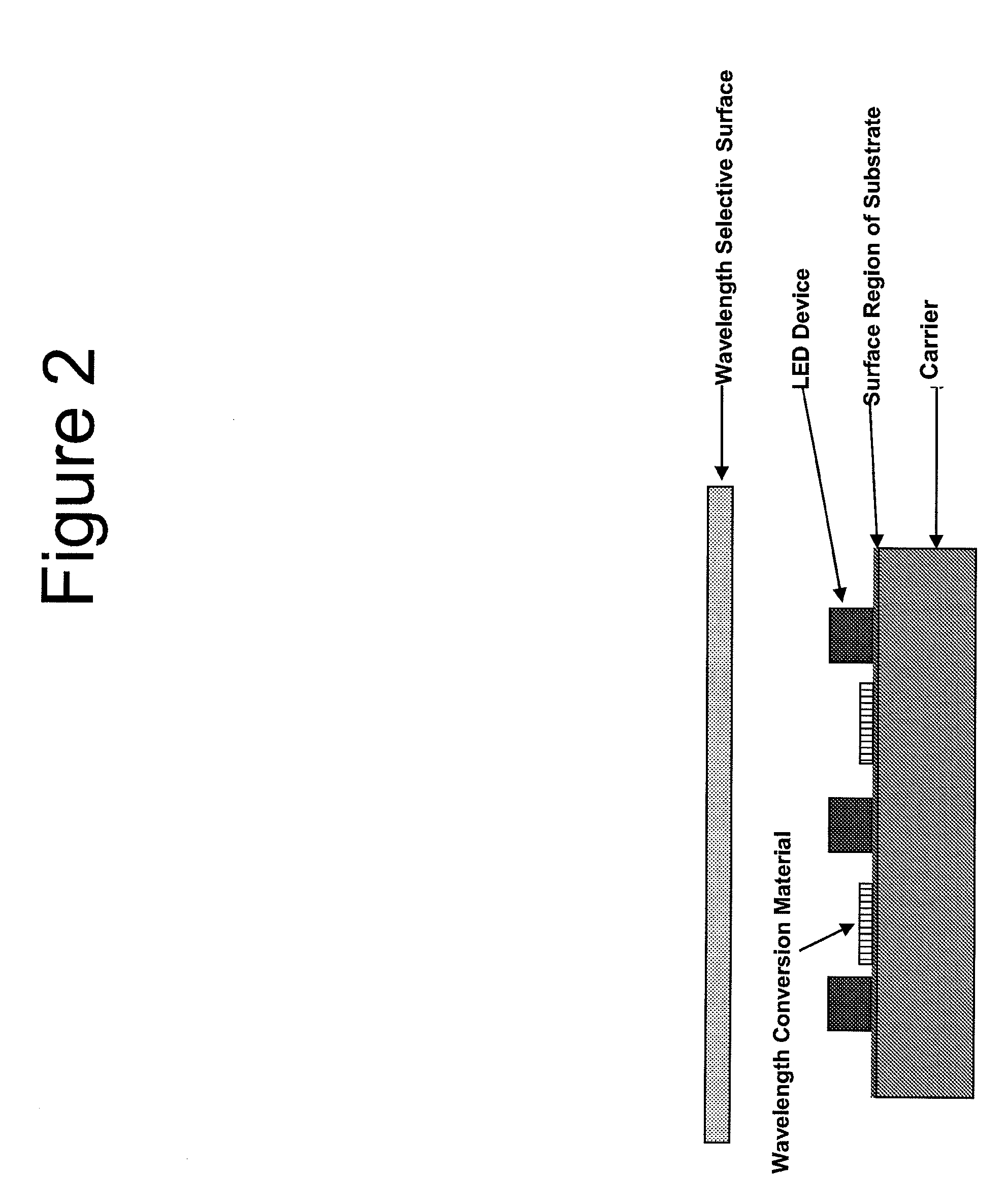
An optical device includes an LED formed on a substrate and a wavelength conversion material, which may be stacked or pixilated, within vicinity of the LED. A wavelength selective surface blocks direct emission of the LED device and transmits selected wavelengths of emission caused by an interaction with the wavelength conversion material.

Description

CROSS-REFERENCE TO RELATED APPLICATIONS[0001]This application claims priority to U.S. Provisional Patent Application No. 61 / 301,183, filed Feb. 3, 2010, commonly assigned and incorporated by reference hereby for all purposes. Also incorporated by reference are commonly assigned patent application Ser. Nos. 12 / 887,207; 12 / 914,789; 61 / 257,303; 61 / 256,934; and 61 / 241,459.BACKGROUND OF THE INVENTION[0002]This invention relates generally to lighting. The invention provides techniques for transmitting electromagnetic radiation from LED devices, such as ultra-violet, violet, blue, blue and yellow, or blue and green. The devices may be fabricated on bulk semipolar or nonpolar materials with use of phosphors, which emit light in a reflection mode. In other embodiments, the starting materials can include polar gallium nitride containing materials. The invention can be applied to white lighting, multi-colored lighting, general illumination, decorative lighting, automotive and aircraft lamps, s...

Claims


Application Information

Patent Timeline
Patent Type & Authority Applications(United States)
IPC IPC(8): H01L33/08B82Y20/00B82Y99/00
CPCH01L33/504H01L33/60H01L2224/48091F21K9/13F21V9/08F21Y2101/02C09K11/0883C09K11/612C09K11/616C09K11/642C09K11/7718C09K11/7721C09K11/7734C09K11/7737C09K11/7738C09K11/7739C09K11/774C09K11/7767C09K11/778C09K11/7784C09K11/7787C09K11/7789C09K11/7792C09K11/7794F21V9/16H01L2924/00014H01L2924/12044F21K9/23F21Y2115/10F21V7/30F21V9/32F21V13/08H01L2924/00
Inventor TROTTIER, TROY ANTHONYKRAMES, MICHAEL RAGANSHARMA, RAJATSHUM, FRANK TIN CHUNGVENKATESH, RAKESH
Owner SORAA
Why Eureka
Try Eureka