Col package having small chip hidden between leads

a semiconductor and lead-side chip technology, applied in semiconductor devices, semiconductor/solid-state device details, electrical equipment, etc., can solve the problems of unbalanced mold flow above and below leads, uneven encapsulant distribution, and affecting mold flow balan

Active Publication Date: 2011-09-08
POWERTECH TECHNOLOGY
View PDF1 Cites 19 Cited by
  • Summary
  • Abstract
  • Description
  • Claims
  • Application Information

AI Technical Summary

Benefits of technology

[0005]The main purpose of the present invention is to provide a Chip-On-Lead (COL) type semiconductor package having small chip hidden b...

Problems solved by technology

When packaging multiple chips within in a COL package, small chips usually cause uneven encapsulant distribu...

Method used


Image

  • Col package having small chip hidden between leads
  • Col package having small chip hidden between leads
  • Col package having small chip hidden between leads

Examples


first embodiment

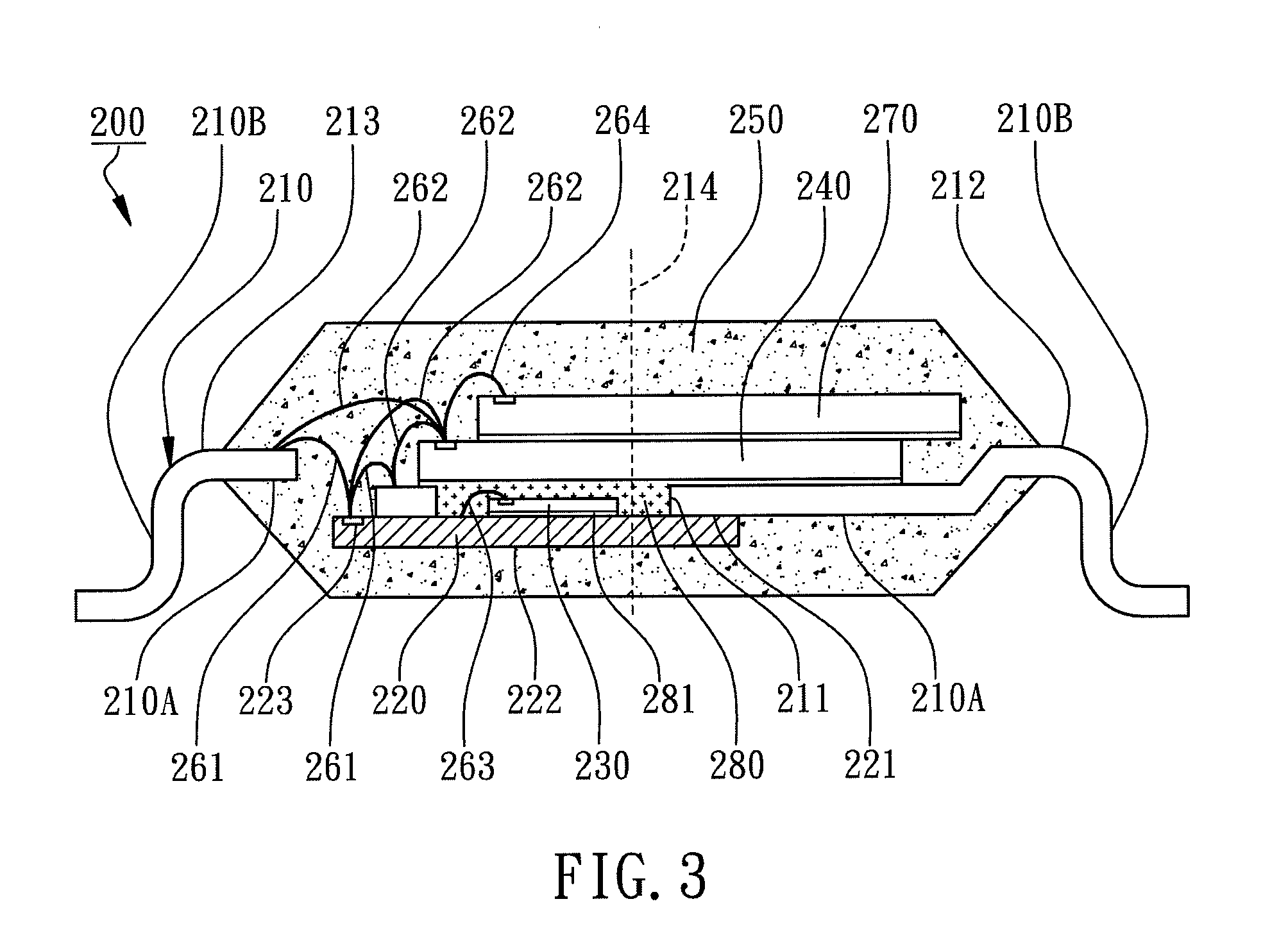
[0018]According to the present invention, a COL type semiconductor package having small chip hidden between leads is illustrated in FIG. 3 for a cross-sectional view and in FIG. 4 for a partial 3D view. The COL type semiconductor package 200 primarily comprises a plurality of leadframe's leads 210, a wiring substrate 220, a first chip 230, a second chip 240, and an encapsulant 250 where the second chip 240 is disposed on the leads 210 and the encapsulant 250 at least encapsulates the second chip 240 to be COL type. Moreover, the COL type semiconductor package 200 conforms to a multi-chip packaging type.

[0019]As shown in FIG. 3, the leads 210 includes a plurality of first side leads 212 and a plurality of second side leads 213 where the first side leads 212 is longer than the second side leads 213 exceeding a central line 214 of the encapsulant 250. The central line 214 is a straight line served as a central line for the COL type semiconductor package 200 which is located at the cent...

second embodiment

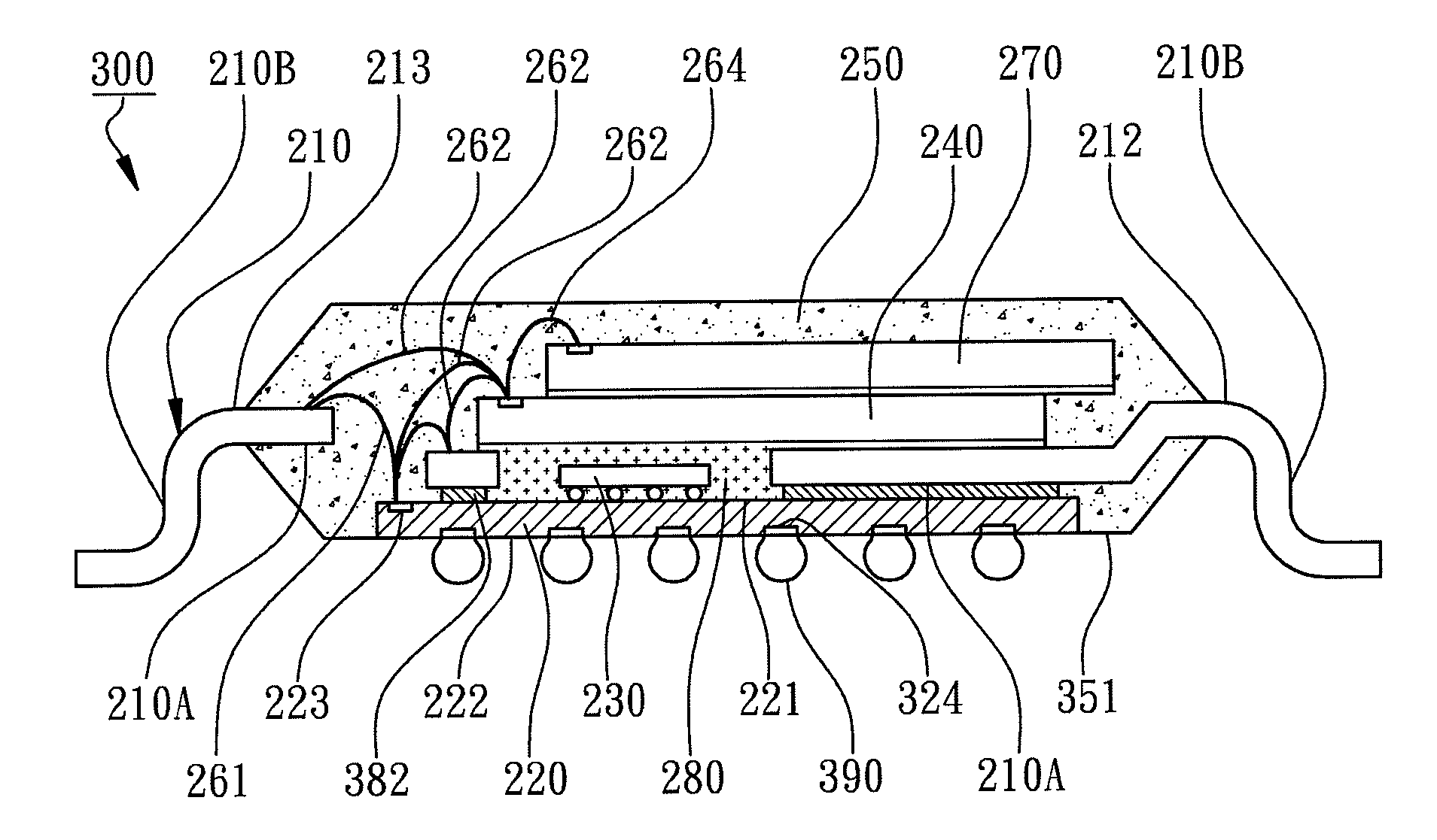
[0026]According to the present invention, another Chip-On-Lead (COL) package having small chip hidden between leads is illustrated in FIG. 6 for a cross-sectional view. The COL type semiconductor package 300 primarily comprises a plurality of leads of a leadframe, a wiring substrate 220, a first chip 230, a second chip 240, and an encapsulant 250 where the major components will be illustrated with the same symbols and numbers which will not be described in detail again.

[0027]The COL type semiconductor package 300 further comprises a plurality of die-attaching adhesive bars 382, such as double-side PI tapes or preform sheets, attached to parts of the bottom surfaces of the first side leads 212 to adhere the top surface 221 of the wiring substrate 220 to the leads 210.

[0028]The first chip 230 is disposed on the top surface 221 of the wiring substrate 220 by passing through the die-holding cavity 221 to keep the first chip 230 on the same disposing level with the leads 210. In the pres...


PUM


Abstract

A Chip-On-Lead (COL) type semiconductor package having small chip hidden between leads is revealed. The lower surfaces of the leadframe's leads are attached to a wiring substrate and the leads are horizontally bent to form a die-holding cavity. A smaller chip is disposed on the wiring substrate by passing through the die-holding cavity to be on the same disposing level with the leads. At least a larger chip is disposed on the leads to overlap the smaller chip so that the small chip does not extrude from the leads. The encapsulant encapsulates a plurality of internal parts of the leads, the wiring substrate, and the larger chip. Therefore, the conventional unbalance issue of mold flow above and below the leads leading to cause excessive warpage can be avoided and numbers of stacked larger chips can be increased to have larger memory capacities.

Description

FIELD OF THE INVENTION[0001]The present invention relates to a semiconductor device, and more particularly to a Chip-On-Lead (COL) type semiconductor package.BACKGROUND OF THE INVENTION[0002]There are various semiconductor packages for semiconductor chips such as TSOP, MSOP and QSOP which are implemented in memory devices or memory cards in consumer electronics. The most popular packages for memory devices are leadframe-based LOC (Lead-On-Chip) packages and COL (Chip-On-Lead) packages where LOC packages including semiconductor chips disposed under the leads are designed for chips with central pads and COL packages including semiconductor chips disposed on top of the leads are designed for chips with peripheral pads. When packaging multiple chips within in a COL package, small chips usually cause uneven encapsulant distribution and affect mold flow balance.[0003]As shown in FIG. 1 and FIG. 2, a conventional COL type semiconductor package 100 comprises a plurality of leadframe's leads...

Claims


Application Information

Patent Timeline
IPC IPC(8): H01L23/495
CPCH01L23/495H01L2224/48091H01L2924/19107H01L2224/73265H01L2224/49175H01L2224/48247H01L2224/32145H01L2924/00014H01L2924/00H01L2924/181H01L2224/05554H01L2224/48145H01L2924/00012H01L23/49575H01L24/48
Inventor WANG, CHIN-FA
Owner POWERTECH TECHNOLOGY
Why Eureka
Try Eureka