Light-Emitting Element and Lighting Device

a technology of light-emitting elements and lighting devices, which is applied in the direction of discharge tubes/lamp details, organic semiconductor devices, discharge tubes/lamp details, etc., can solve the problems of limiting and achieve the improvement of power efficiency of the whole light-emitting element, high power efficiency, and improved power efficiency

Active Publication Date: 2011-09-08
SEMICON ENERGY LAB CO LTD
View PDF11 Cites 188 Cited by
  • Summary
  • Abstract
  • Description
  • Claims
  • Application Information

AI Technical Summary

Benefits of technology

[0013]In view of the above, the top-priority object of one embodiment of the present invention is to improve power efficiency. Another object is to provide a light-emitting element which emits light of color which is not necessarily white but is natural color like light bulb color or warm white. Another object is to provide a lighting device including the light-emitting element as a light source.
[0030]The above light-emitting element emits light of natural color like light bulb color or warm white, and thus can be used as a light source of an indoor lighting device or an outdoor lighting device. The use of the above light-emitting element makes it possible to provide lighting devices which have high power efficiency and consume less power.

Problems solved by technology

For that reason, there was a limit to improvement in power efficiency.

Method used


Image

  • Light-Emitting Element and Lighting Device
  • Light-Emitting Element and Lighting Device
  • Light-Emitting Element and Lighting Device

Examples


embodiment 1

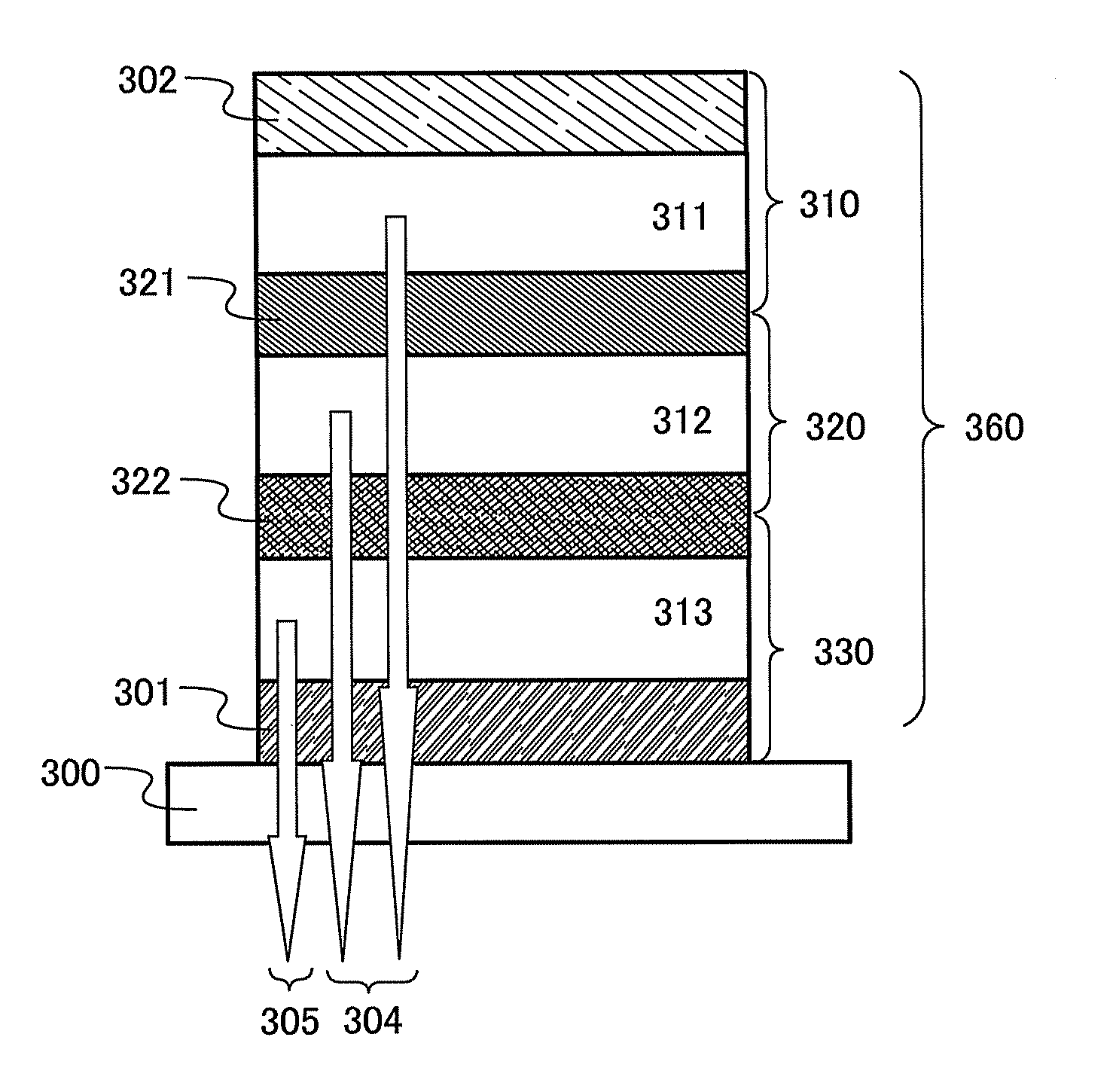
[0060]In this embodiment, an example of a structure of a light-emitting element will be described with reference to FIG. 1, FIG. 2, FIG. 3, FIG. 4, and FIG. 5.

[0061]A light-emitting element 360 illustrated in FIG. 1 is provided over a substrate 300 and includes an anode 301 and a cathode 302, and a first light-emitting layer 311, a second light-emitting layer 312, a third light-emitting layer 313, a first intermediate layer 321, and a second intermediate layer 322 between the anode 301 and the cathode 302. The first intermediate layer 321 is provided between the first light-emitting layer 311 and the second light-emitting layer 312. The second intermediate layer 322 is provided between the second light-emitting layer 312 and the third light-emitting layer 313. A first light-emitting unit 310 includes the cathode 302, the first light-emitting layer 311, and the first intermediate layer 321. A second light-emitting unit 320 includes the first intermediate layer 321, the second light-e...

embodiment 2

[0083]In this embodiment, an example of a structure of a light-emitting element will be described with reference to FIG. 1. In this embodiment, the structure of the light-emitting element 360 illustrated in FIG. 1, which is described in Embodiment 1, will be specifically described.

[0084]As described in Embodiment 1, the light-emitting element 360 illustrated in FIG. 1 is provided over the substrate 300 and includes the anode 301 and the cathode 302, and the first light-emitting layer 311, the second light-emitting layer 312, the third light-emitting layer 313, the first intermediate layer 321, and the second intermediate layer 322 between the anode 301 and the cathode 302. The first intermediate layer 321 is provided between the first light-emitting layer 311 and the second light-emitting layer 312. The second intermediate layer 322 is provided between the second light-emitting layer 312 and the third light-emitting layer 313. The first light-emitting unit 310 includes the cathode 3...

example 1

[0111]In this example, a light-emitting element that is one embodiment of the present invention will be described with reference to FIG. 6, FIG. 9, FIG. 10, FIG. 11, FIG. 12, and FIG. 13. In addition, a comparative element 1 will be described with reference to FIG. 7, FIG. 9, FIG. 10, FIG. 11, FIG. 12, and FIG. 13. In addition, a comparative element 2 will be described with reference to FIG. 8, FIG. 9, FIG. 10, FIG. 11, FIG. 12, and FIG. 13. Chemical formulae of materials used in this example are shown below.

[0112]Manufacturing methods of a light-emitting element 1 of this example, the comparative element 1, and the comparative element 2 will be described below.

[0113]First, the light-emitting element 1 will be described (see FIG. 6). Indium tin oxide containing silicon oxide was deposited by a sputtering method over a glass substrate 500 to form an anode 501. The thickness of the anode 501 was 110 nm and the electrode area was 2 mm×2 mm.

[0114]Next, the substrate on which the anode 5...


PUM


Abstract

To provide a light-emitting element whose power efficiency is improved and which emits light of natural color like light bulb color. In the light-emitting element, at least three light-emitting units are stacked. The emission spectrum of the light-emitting element has two peaks. One of the two peaks is obtained by combining spectra of light emitted from two light-emitting units. The peak is in the yellow to orange wavelength range and has a wavelength greater than or equal to 560 nm and less than 580 nm. Thus, a wavelength range of high luminosity can be used and the power efficiency can be improved. The color of light emitted from the light-emitting element is close to a blackbody locus in a chromaticity diagram, and light of natural color like light bulb color can be achieved.

Description

BACKGROUND OF THE INVENTION[0001]1. Field of the Invention[0002]The present invention relates to a light-emitting element utilizing electroluminescence. The present invention also relates to a light-emitting device or a lighting device which includes the light-emitting element.[0003]2. Description of the Related Art[0004]In recent years, research and development have been actively conducted on light-emitting elements utilizing electroluminescence. In a basic structure of the light-emitting element utilizing electroluminescence, a layer containing a light-emitting substance (hereinafter, the layer is referred to as a “light-emitting layer”) is sandwiched between a pair of electrodes. By applying voltage between the pair of electrodes of the light-emitting element, light can be emitted from the light-emitting substance.[0005]Among light-emitting elements utilizing electroluminescence, a light-emitting element in which an organic compound is used as a light-emitting substance can be fo...

Claims


Application Information

Patent Timeline
Patent Type & Authority Applications(United States)
IPC IPC(8): H01J1/62
CPCC09K11/06H05B33/14C09K2211/1011C09K2211/1014C09K2211/1029C09K2211/1044C09K2211/185H01L27/3209H01L51/0059H01L51/006H01L51/0085H01L51/5016H01L51/5278H01L2251/5361C09K2211/1007H10K59/32H10K85/631H10K85/633H10K85/342H10K50/11H10K2101/10H10K50/19Y02B20/30
Inventor SEO, SATOSHIUSHIKUBO, TAKAHIRO
Owner SEMICON ENERGY LAB CO LTD
Why Eureka
Try Eureka