Optical Modulators With Controllable Chirp

a technology of optical modulators and chirps, applied in the field of optical modulators, can solve the problems of silicon-based optical modulators in general, lithium niobate-based optical devices have inherent performance limitations, and the use of lithium niobate-based devices in such a situation is not an option, and achieves the effect of small capacitance load

Inactive Publication Date: 2011-09-15
CISCO TECH INC
View PDF9 Cites 20 Cited by
  • Summary
  • Abstract
  • Description
  • Claims
  • Application Information

AI Technical Summary

Benefits of technology

[0017]The phase modulation control section may be located within the modulator itself (with one segment on each arm, driven by the same input signal), or may be disposed “outside” of the modulator on either the input waveguiding section or the output waveguiding section. The placement of the phase modulation control section on the “outside” of the modulator having the advantage of creating a smaller capacitive load for the driver circuitry. The length of the phase modulation control section (in conjunction with the drive voltage applied to provide the modulation) then defines the amount of optical phase introduced to the propagating signal. It is important that when located inside the modulator, the segments are driven by the same polarity signal so that both segments impart the same phase delay to the signals propagating along each arm without creating a net phase difference between the two modulated signals as they are re-combined at the output of the modulator.

Problems solved by technology

Clearly, the use of lithium niobate-based optical devices in such a situation is not an option.
Moreover, it is well-known that lithium niobate-based devices have inherent performance limitations at data rates exceeding, for example, 1 GB / s, since they need to be modeled as traveling wave structures, with relatively complex electrical drive structures required to attempt to have the device operate at the requisite speed.
While considered a significant advance in the state of the art over lithium niobate modulators, silicon-based optical modulators in general and the exemplary configuration of FIG. 3 in particular are known to suffer from chirp as a result of the inherent phase response and optical loss differences between the two arms of the modulator.
Chirp is a time-varying optical phase that can be detrimental to the transmission behavior of an optical signal as it propagates through dispersive fiber.

Method used


Image

  • Optical Modulators With Controllable Chirp
  • Optical Modulators With Controllable Chirp
  • Optical Modulators With Controllable Chirp

Examples


Embodiment Construction

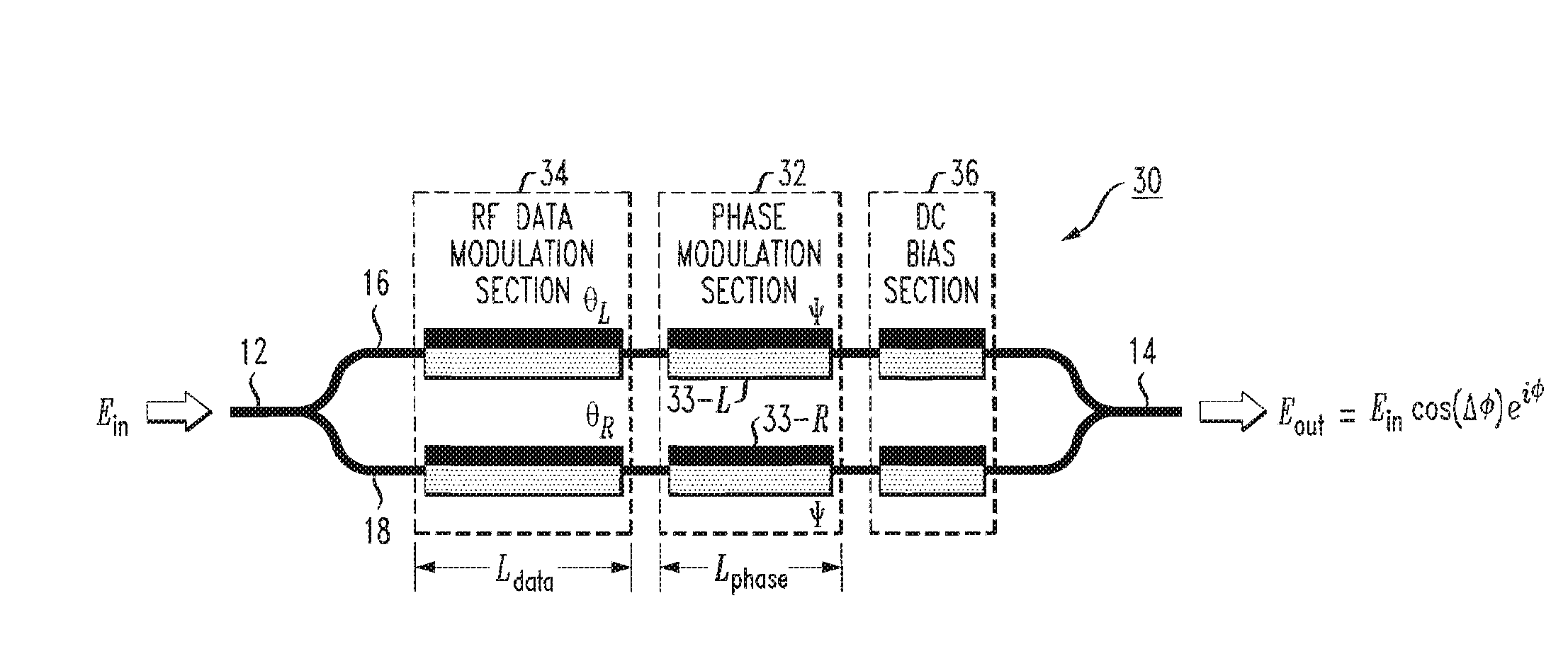
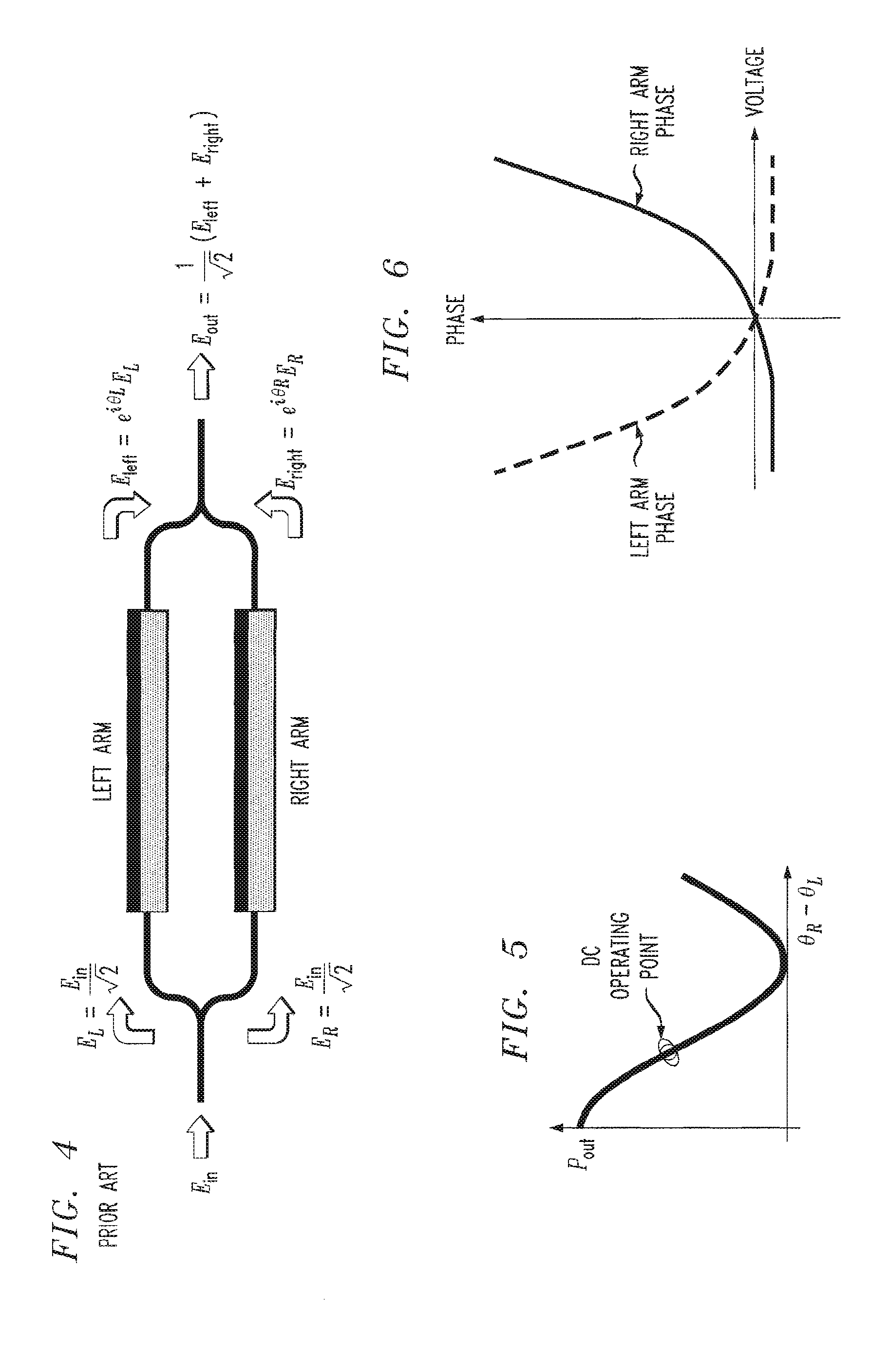
[0037]FIG. 7 illustrates an exemplary chirp controlled optical modulator 30 formed in accordance with the present invention. For the purposes of discussion, the components of modulator 30 that are similar to components of prior art modulator 10 carry the same reference numerals and their functionality is not discussed in detail. In this particular embodiment of the present invention, a phase modulation control section 32 is included in modulator 30 and is located “inside” the modulator with RF data modulation section 34 (which functions in the manner of the prior art as described above to impress an electrical modulating input signal on a CW optical signal propagating through the structure). In the embodiment of FIG. 7, a separate DC bias section 36 is also shown. The use of DC bias in a modulator is well-known in the art, and is used to ensure that the modulator provides the desired phase shift around a specific operating point. The DC operating point is shown on FIG. 5 as preferab...


PUM

PropertyMeasurementUnit
conductivity typeaaaaaaaaaa
lengthaaaaaaaaaa
phaseaaaaaaaaaa

Abstract

A semiconductor-based optical modulator is presented that includes a separate phase control section to adjust the amount of chirp present in the modulated output signal. At least one section is added to the modulator configuration and driven to create a pure “phase” signal that will is added to the output signal and modify the e term inherent in the modulation function. The phase modulation control section may be located within the modulator itself (with one segment on each arm, driven by the same input signal), or may be disposed “outside” of the modulator on either the input waveguiding section or the output waveguiding section. The phase control section may be formed to comprise multiple segments (of different lengths), with the overall phase added to the propagating signal controlled by selecting the different segments to be energized to impart a phase delay to a signal propagating through the energized section(s).

Description

CROSS-REFERENCE TO RELATED APPLICATIONS[0001]This application claims the benefit of U.S. Provisional Application No. 61 / 312,285, filed Mar. 10, 2010 and herein incorporated by reference.TECHNICAL FIELD[0002]The present invention relates to optical modulators and, more particularly, to semiconductor-based optical modulators including a separate phase control segment to adjust the amount of chirp present in the modulated output signal.BACKGROUND OF THE INVENTION[0003]For many years, optical modulators have been made out of electro-optic material, such as lithium niobate. Optical waveguides are formed within the electro-optic material, with metal contact regions disposed on the surface of each waveguide arm. A continuous wave (CW) optical signal is launched into the waveguide, and an electrical data signal input is applied as an input to the metal contact regions. The applied electrical signal modifies the refractive index of the waveguide region underneath the contact, thus changing t...

Claims


Application Information

Patent Timeline
Patent Type & Authority Applications(United States)
IPC IPC(8): G02F1/035
CPCG02F1/2257G02F2203/20G02F1/025G02F2203/255G02F2203/25
Inventor WEBSTER, MARKSHASTRI, KALPENDU
Owner CISCO TECH INC
Why Eureka
Try Eureka