Sram-type memory cell

a memory cell and sram technology, applied in the field of sram-type memory cells, can solve the problems of limiting the margin for improvement of the various functional modes, and the choice of working in the well column does not favour the facilitation of the operating mode,

Active Publication Date: 2011-09-29
S O I TEC SILICON ON INSULATOR THECHNOLOGIES
View PDF85 Cites 15 Cited by
  • Summary
  • Abstract
  • Description
  • Claims
  • Application Information

AI Technical Summary

Benefits of technology

[0044]FIG. 6 illustrates the modalities controlling the thresh

Problems solved by technology

However, in these devices, the back control gate simply comprises a well which is limited by the isolating trench.
Moreover, the choice of working in columns of wells does not favour the facilitation of the operating modes.
For example, the article by Yama

Method used


Image

  • Sram-type memory cell
  • Sram-type memory cell
  • Sram-type memory cell

Examples


Embodiment Construction

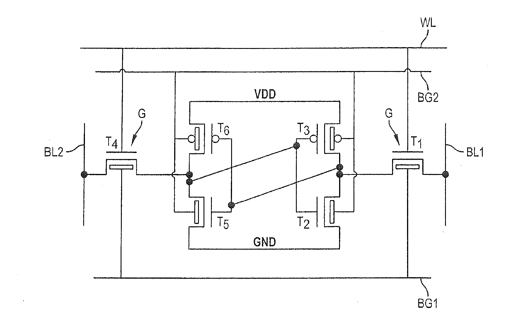
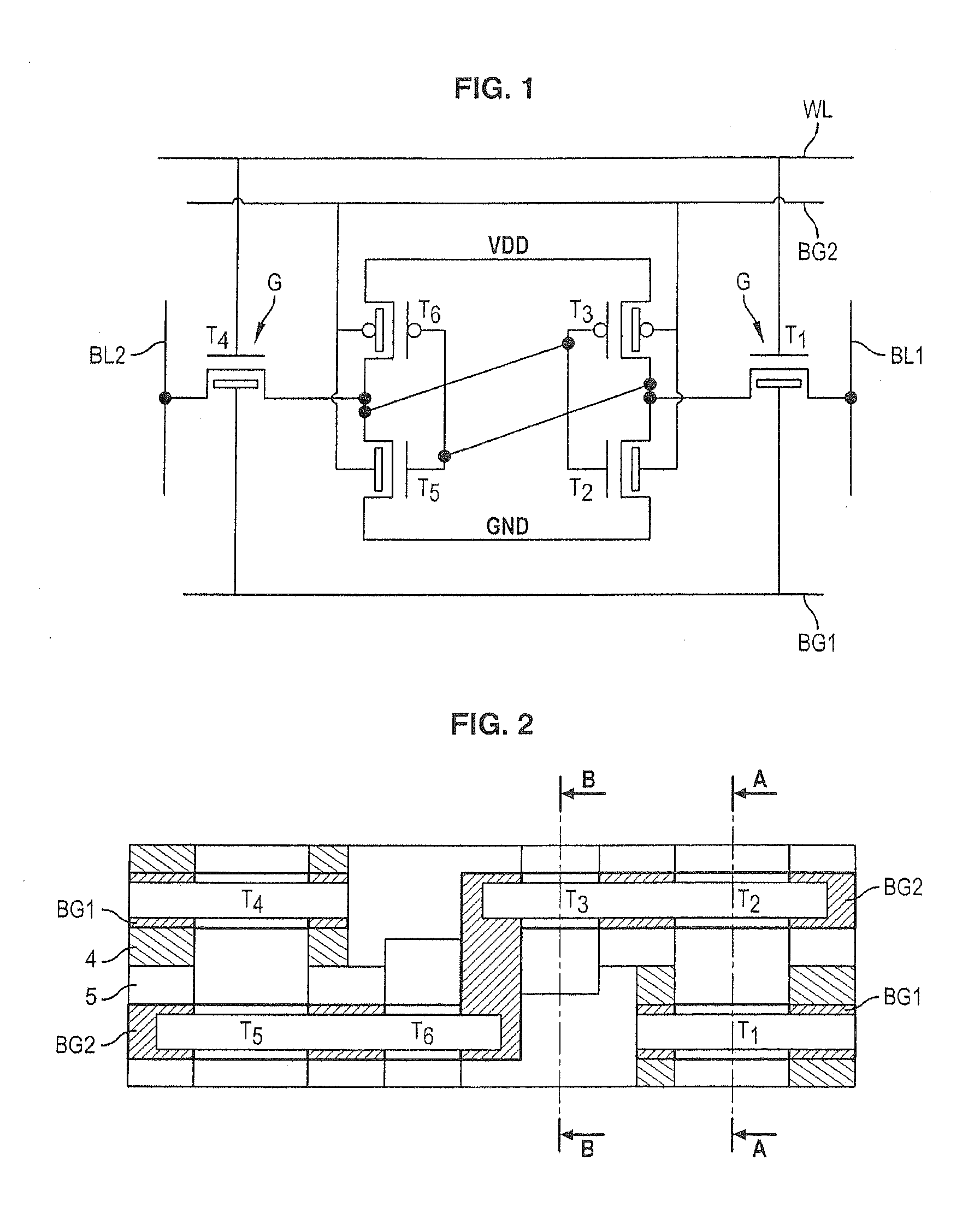
[0045]Structure of the SRAM Cell

[0046]FIG. 1 shows the circuit diagram corresponding to an SRAM-type memory cell according to the invention.

[0047]The memory cell comprises six transistors T1 to T6.

[0048]Two of these transistors are access transistors T1 and T4.

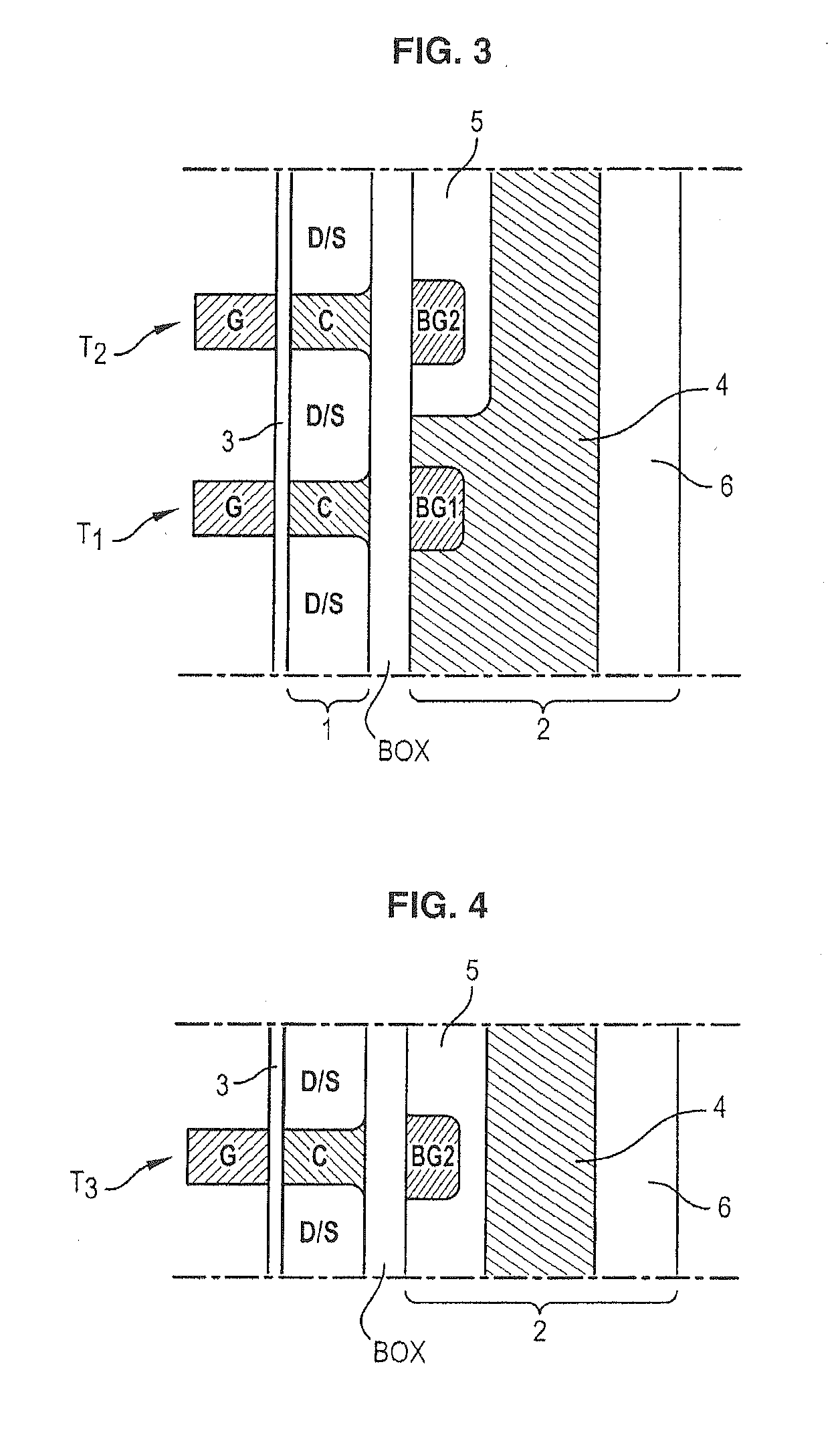
[0049]The transistors T1 and T4 are produced on a semiconductor on insulator substrate and each of the transistors has a front gate G and a back control gate BG1 that can be controlled to modify the behaviour of the transistor.

[0050]Preferably a back gate line is used to collectively connect the back control gate BG1 of the two access transistors T1, T4 to one and the same potential, which makes it possible to provide easy and inexpensive control, but it is also possible for each of the back gates to be individually connected to a potential.

[0051]The front gate G of each of the access transistors T1 and T4 is linked to a word line WL.

[0052]Moreover, a drain electrode of each of the access transistors T1 and T4 is linked to a b...


PUM


Abstract

An SRAM-type memory cell that includes a semiconductor on insulator substrate having a thin film of semiconductor material separated from a base substrate by an insulating layer; and six transistors such as two access transistors, two conduction transistors and two charge transistors arranged so as to form with the conduction transistors two back-coupled inverters. Each of the transistors has a back control gate formed in the base substrate below the channel and able to be biased in order to modulate the threshold voltage of the transistor, with a first back gate line connecting the back control gates of the access transistors to a first potential and a second back gate line connecting the back control gates of the conduction transistors and charge transistors to a second potential. The first and second potentials can be modulated according to the type of cell control operation.

Description

FIELD OF THE INVENTION[0001]The present invention relates to an SRAM-type memory cell formed on a semiconductor on insulator substrate and comprising six transistors.BACKGROUND OF THE INVENTION[0002]SRAM (“Static Random Access Memory”) type memory cells are static ram memories, that is to say memories that do not require periodic refreshing.[0003]Such memory cells are constructed from a set of transistors.[0004]A general concern in this field is how to reduce the size of the cells and how to reduce the leakage currents.[0005]When an SRAM cell is fabricated on a bulk substrate, the size reduction results in a greater variability, which means that the dimensions of the transistors must not be reduced too much, and the read and write components must be separated in order to find an operating point.[0006]This may entail increasing the number of transistors (thus increasing from 6 to 8, or even 10 transistors), with an attendant penalty in terms of surface area.[0007]Moreover, on a “bulk...

Claims


Application Information

Patent Timeline
IPC IPC(8): H01L27/092H01L21/28
CPCG11C11/412H01L27/1203H01L27/1104H01L21/84H10B10/12H10B99/00H10B10/00
Inventor MAZURE, CARLOSFERRANT, RICHARDNGUYEN, BICH-YEN
Owner S O I TEC SILICON ON INSULATOR THECHNOLOGIES
Why Eureka
Try Eureka