Semiconductor device package and method of fabricating the same

a technology of semiconductor devices and semiconductor devices, applied in the direction of semiconductor devices, semiconductor/solid-state device details, electrical equipment, etc., can solve the problems of easy damage to the semiconductor device package, the requirement for the functionality of products getting higher among consumers, and the yield and quality of the relative products are improved, so as to avoid damage to the chip

Active Publication Date: 2011-09-29
ADVANCED SEMICON ENG INC
View PDF8 Cites 56 Cited by
  • Summary
  • Abstract
  • Description
  • Claims
  • Application Information

AI Technical Summary

Benefits of technology

[0006]It is therefore an object of the invention to provide a semiconductor device package and a method of fabricating the same. The semiconductor device package has a buffer structure for controlling the gap between the chip and the substrate and absorbing the impact to the chip, which avoids damages to the chip and thus improves the yield and quality of the relative products.

Problems solved by technology

However, even so the yield and quality of semiconductor-related products remain limited, and the requirement for the functionality of the products is getting higher among the consumers.
On the manufacturing process, a semiconductor device package is easily damaged due to cracks in the chips of the package when the chips are subjected to stress.
The flaws of chips are mostly caused by the process gadgets or because of the fragile feature of the chip structure.

Method used


Image

  • Semiconductor device package and method of fabricating the same
  • Semiconductor device package and method of fabricating the same
  • Semiconductor device package and method of fabricating the same

Examples


Embodiment Construction

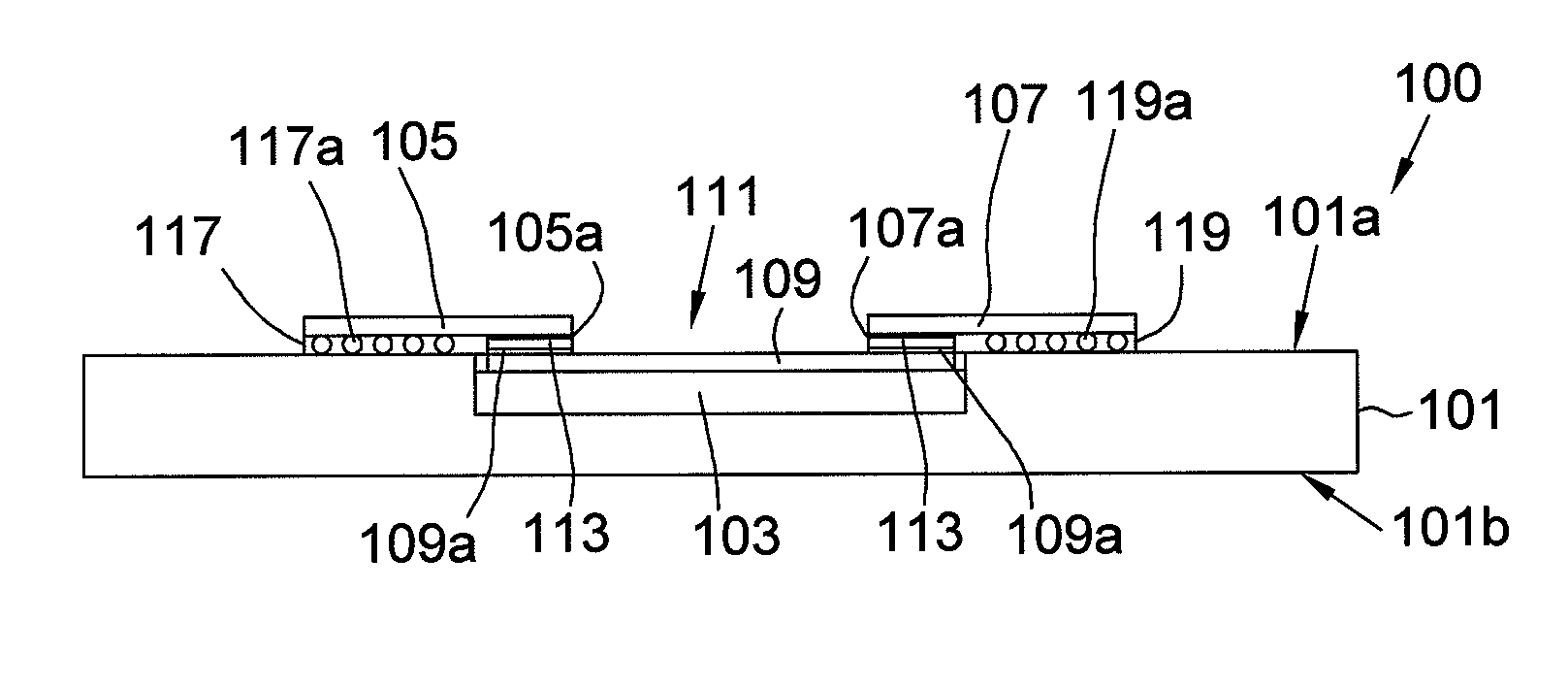
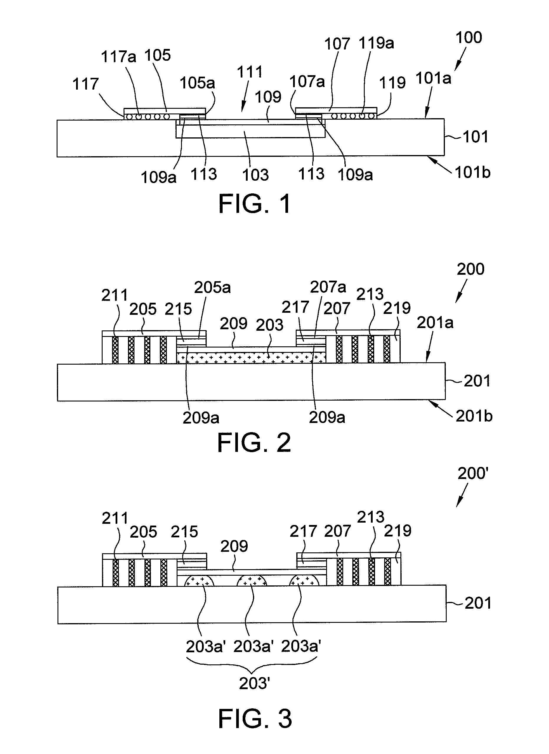
[0017]FIG. 1 shows a semiconductor device package according to a preferred embodiment of the invention. The semiconductor device package 100 includes a substrate 101, a buffer structure 103, two active chips 105, 107 and a bridge chip 109. The substrate 101 has a cavity 111, a first surface 101a and a second surface 101b opposite to the first surface 101a. The cavity 111 is extended from the first surface 101a toward the second surface 101b, and the buffer structure 103 is disposed in the cavity 111. The active chips 105 and 107 are mechanically and electrically connected to the first surface 101a and around the cavity 111. The active chips 105 and 107 both have an active surface. The bridge chip 109 is disposed in the cavity 111 and above the buffer structure 103. The bridge chip 109 has an active surface that faces the active surfaces of the active chips 105 and 107 and is partially overlapped with the active surfaces of the active chips 105 and 107. Therefore, the bridge chip 109...


PUM


Abstract

A semiconductor device package and a method of fabricating the same are disclosed. The semiconductor device package includes a substrate, a buffer structure, two active chips and a bridge chip. The substrate has a cavity, a first surface and a second surface opposite to the first surface. The cavity is extended from the first surface toward the second surface, and the buffer structure is disposed in the cavity. The active chips are mechanically disposed on and electrically connected to the first surface and around the cavity, wherein the active chips both have a first active surface. The bridge chip is disposed in the cavity and above the buffer structure, wherein the bridge chip has a second active surface, the second active surface faces the first active surfaces and is partially overlapped with the first active surfaces, the bridge chip is used for providing a proximity communication between the active chips.

Description

BACKGROUND OF THE INVENTION[0001]1. Field of the Invention[0002]The invention relates in general to a device package, and more particularly to a semiconductor device package.[0003]2. Description of the Related Art[0004]Nowadays, the semiconductor technology has been applied to uncountable products including memory cards, computers, mobile phones, monitors, etc. The semiconductor manufacturing process requires accuracy because of the miniature size and delicate structure of the semiconductor components, thus each step during the process is strictly monitored and controlled in case of mistakes happening. However, even so the yield and quality of semiconductor-related products remain limited, and the requirement for the functionality of the products is getting higher among the consumers.[0005]On the manufacturing process, a semiconductor device package is easily damaged due to cracks in the chips of the package when the chips are subjected to stress. The flaws of chips are mostly cause...

Claims


Application Information

Patent Timeline
Patent Type & Authority Applications(United States)
IPC IPC(8): H01L23/488H01L21/60
CPCH01L21/563H01L23/48H01L2924/07811H01L2924/014H01L2924/01075H01L2924/01006H01L2224/131H01L2924/01082H01L2924/01079H01L2924/01047H01L2924/01033H01L2924/01029H01L2224/97H01L2224/92242H01L2224/92143H01L2224/73204H01L2224/73203H01L23/5389H01L23/562H01L24/73H01L24/92H01L24/97H01L25/0652H01L25/0655H01L2224/13139H01L2224/13144H01L2224/13147H01L2224/30155H01L2224/30181H01L2224/73103H01L2224/73153H01L2924/00014H01L2924/01014H01L2924/00
Inventor CHANG, HSIAO-CHUANTSAI, TSUNG-YUEHLAI, YI-SHAOCHENG, MING-HSIANG
Owner ADVANCED SEMICON ENG INC
Why Eureka
Try Eureka