Switching device driving unit and semiconductor apparatus

a driving unit and switching device technology, applied in the direction of power conversion systems, oscillation generators, pulse techniques, etc., can solve the problems of affecting the operation of the switching device, and the switching device and the driving unit are not reliable enough. to achieve the effect of suppressing the variation in the slew rate of the output voltag

Inactive Publication Date: 2011-10-06
PANASONIC CORP
View PDF1 Cites 54 Cited by
  • Summary
  • Abstract
  • Description
  • Claims
  • Application Information

AI Technical Summary

Benefits of technology

In order to solve the above-mentioned problems with the conventional switching device driving unit, the present invention relates to a switching device driving unit that drives a switching device in which a gate current is allowed to flow upon application of a bias voltage to a gate, such as an FET in which a p-type region or a Schottky electrode is used for a gate, and an object thereof is to provide a switching device driving unit and a semiconductor apparatus which, even in a case where the threshold voltage

Problems solved by technology

Therefore, in a case where the constant-current driving operation is continued as it is even after completion of a transition state of the switching device 50 from the ON state to the OFF state, or from the OFF state to the ON state, a great voltage in a forward direction or in a reverse direction is applied to the gate terminal of the switching device 50 to cause damages to a gate oxide film of the switching device 50, resulting in degradation of reliability of the device.
However, in a case where-there is used, as the switching device driven by the conventional switching device driving unit shown in FIG. 6, a switching device in which a gate current or a base current is allowed to flow upon application of a bias voltage to a gate or a base, such as an FET in which a p-type region or a Schottky electro

Method used


Image

  • Switching device driving unit and semiconductor apparatus
  • Switching device driving unit and semiconductor apparatus
  • Switching device driving unit and semiconductor apparatus

Examples


first embodiment

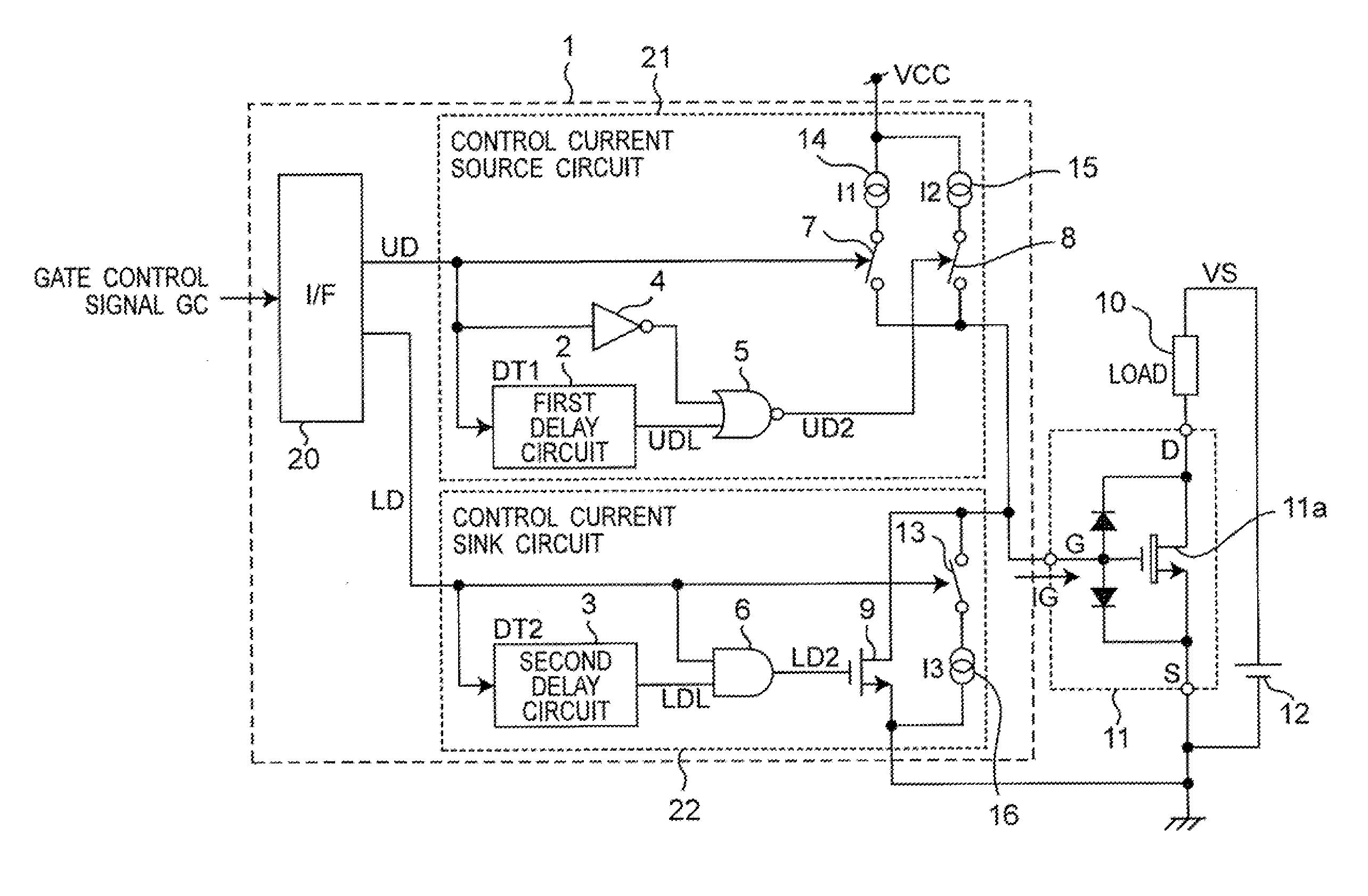
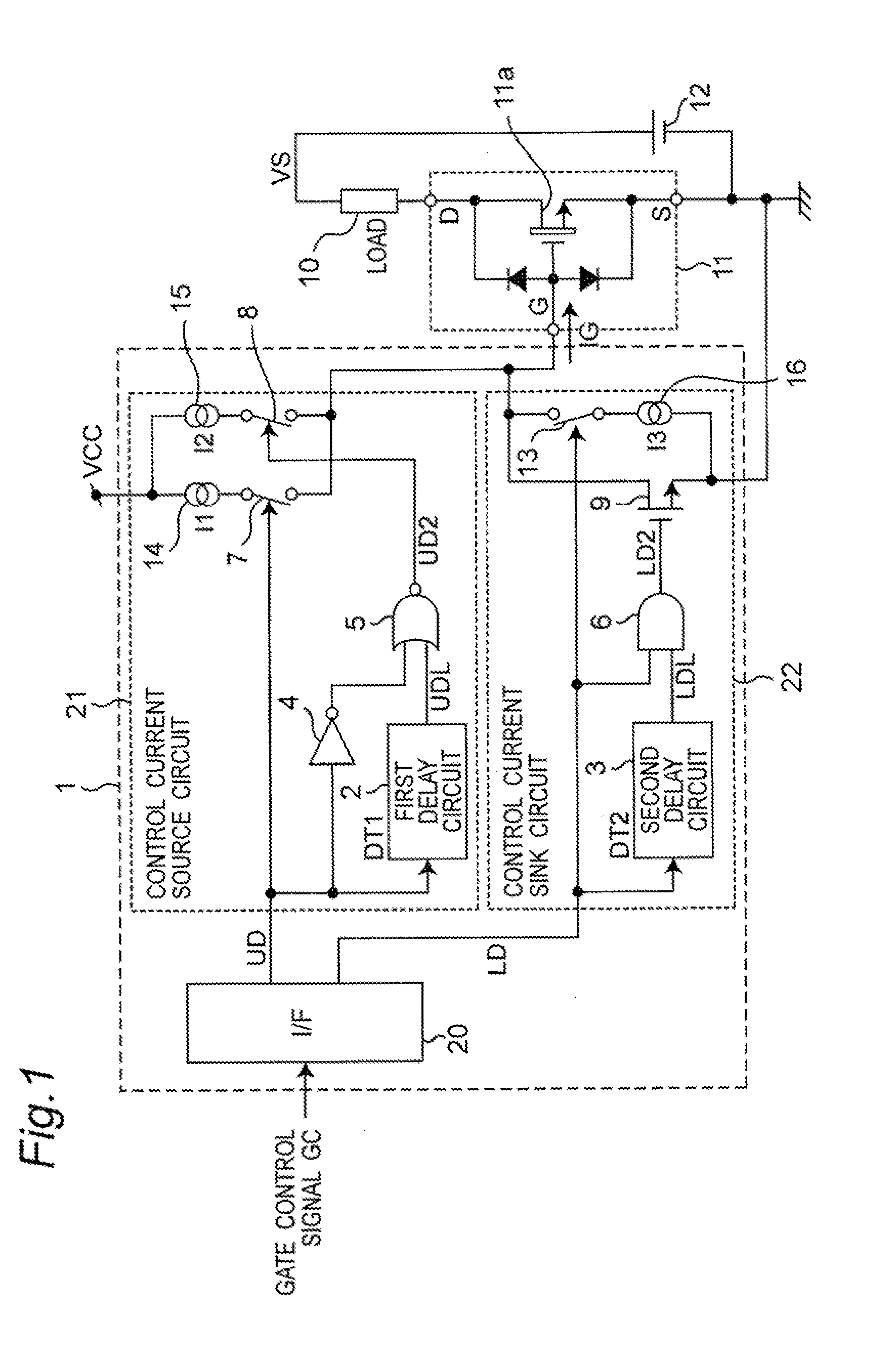
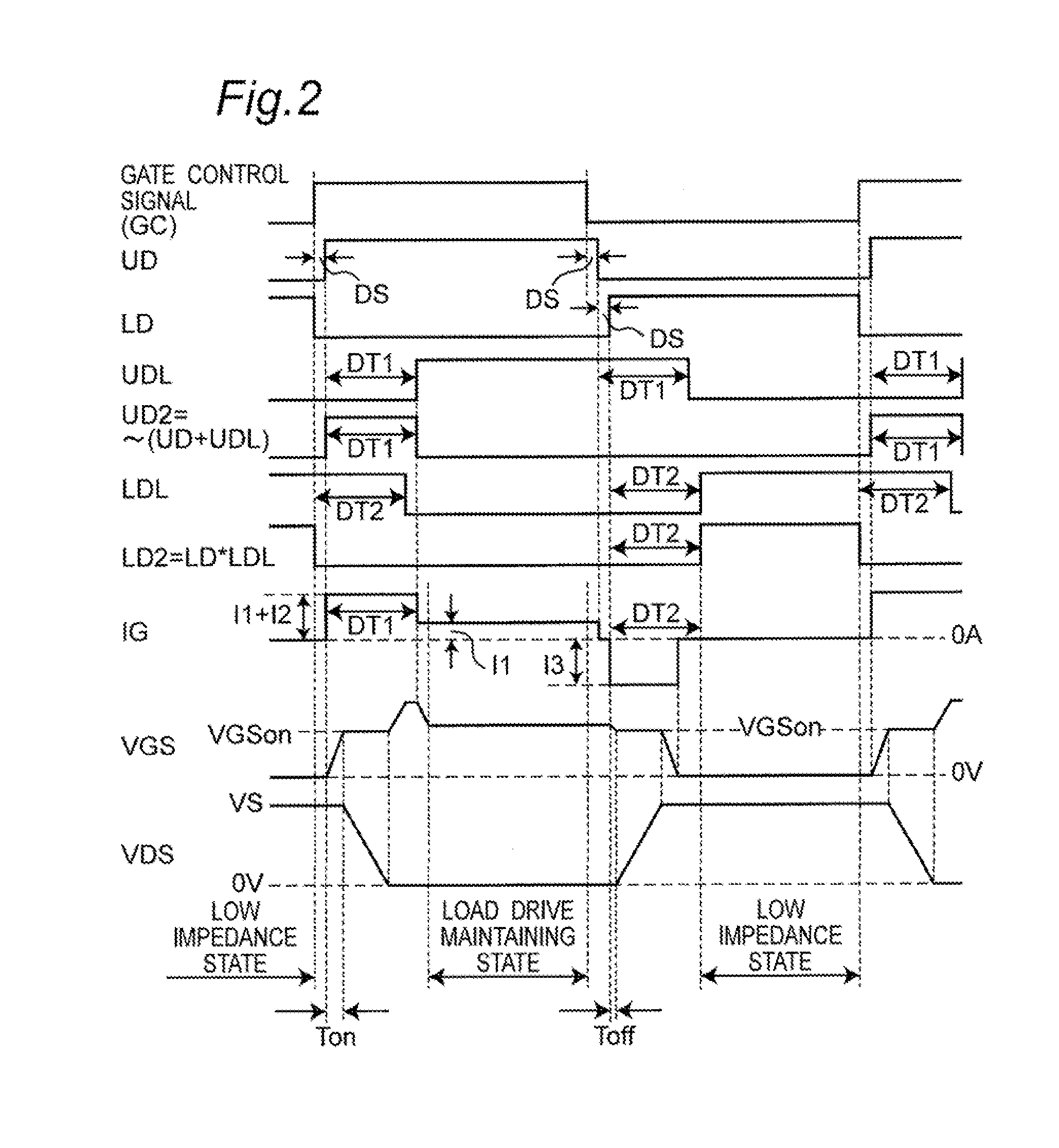
FIG. 1 is a block diagram that illustrates a specific structure of a first embodiment of a switching device driving unit and a semiconductor apparatus in accordance with the present invention. Referring to FIG. 1, the following description will discuss the first embodiment of the switching device driving unit in accordance with the present invention.

A switching device driving unit 1, which ON / OFF drives (carries out switching operations) a switching device 11, is constituted by an I / F (interface) circuit 20 to which a gate control signal (GC) is inputted, a control current source circuit 21 to which a signal (US) is inputted from the I / F circuit 20 and which is connected to a power supply side (VCC) , and a control current sink circuit 22 to which a signal (LD) is inputted from the I / F circuit 20 and which is connected to a ground. Outputs from the control current source circuit 21 and the control current sink circuit 22 are inputted to a gate terminal (G) of the switching device 11...

second embodiment

FIG. 4 is a block diagram that illustrates a specific structure of a second embodiment of a switching device driving unit and a semiconductor apparatus in accordance with the present invention. Referring to FIG. 4, the following description will discuss the second embodiment of a switching device driving unit and a semiconductor apparatus in accordance with the present invention. In the description of the switching device driving unit and semiconductor apparatus of the second embodiment, those members having the same functions and structures as those of the switching device driving unit and semiconductor apparatus of the first embodiment are indicated by the same reference numerals, and the description thereof will not be repeated.

A switching device driving unit 30, which ON / OFF drives (carries out switching operations) a switching device 11, is constituted by an I / F (interface) circuit 31 to which a gate control signal (GC) is inputted, a control current source circuit 40 to which ...


PUM


Abstract

In order to provide a switching device driving unit that, even in a case where a threshold voltage of a switching device is varied, can suppress variations in switching speed, and prevent a power loss caused by an unnecessary gate current in a constant ON operation state of the switching device, so that a desired slew rate can be easily set, a control current source circuit sets to different values based on a first input driving signal, in a driving current to be source-outputted to a gate or a base of the switching device, a current in a stage of an initial ON operation of a switching operation of the switching device and a current in a stage after completion of the switching operation.

Description

FIELD OF THE INVENTIONThe present invention relates to a switching device driving unit for drive-controlling a switching device to be installed in a semiconductor integrated circuit apparatus or the like, and to a semiconductor apparatus, and more particularly concerns such a switching device driving unit for drive-controlling (switch-driving) a switching device that allows a gate current or a base current to flow upon application of a bias voltage to a gate or a base, such as an FET in which a p-type region or a Schottkyelectrode is used for a gate, or a bipolar transistor, and to a semiconductor apparatus.BACKGROUND OF THE INVENTIONFIG. 6 is a block diagram that illustrates a conventional switching device driving unit disclosed in Japanese Unexamined Patent Publication No. 2009-11049.The conventional switching device driving unit shown in FIG. 6 is suitably used for switch-driving a switching device with a gate terminal serving as a control terminal for an IGBT or MOS transistor b...

Claims


Application Information

Patent Timeline
IPC IPC(8): H03K17/00
CPCH02M1/08H03K17/164H03K17/145
Inventor TAMAOKA, SHUJI
Owner PANASONIC CORP
Why Eureka
Try Eureka