

Touch display panel
a technology of touch display and display panel, which is applied in the direction of instruments, computing, electric digital data processing, etc., can solve the problems of increasing fabrication costs and complicating the fabrication process of electronic products, and achieve the effect of improving the manufacturing process and improving the manufacturing efficiency
- Summary
- Abstract
- Description
- Claims
- Application Information
AI Technical Summary
Benefits of technology
Problems solved by technology
Method used
Image

Examples
first embodiment
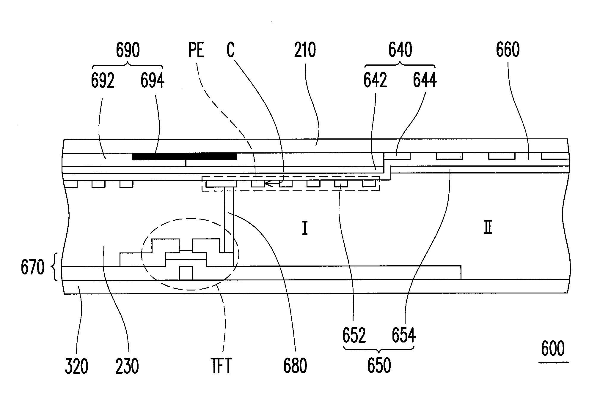
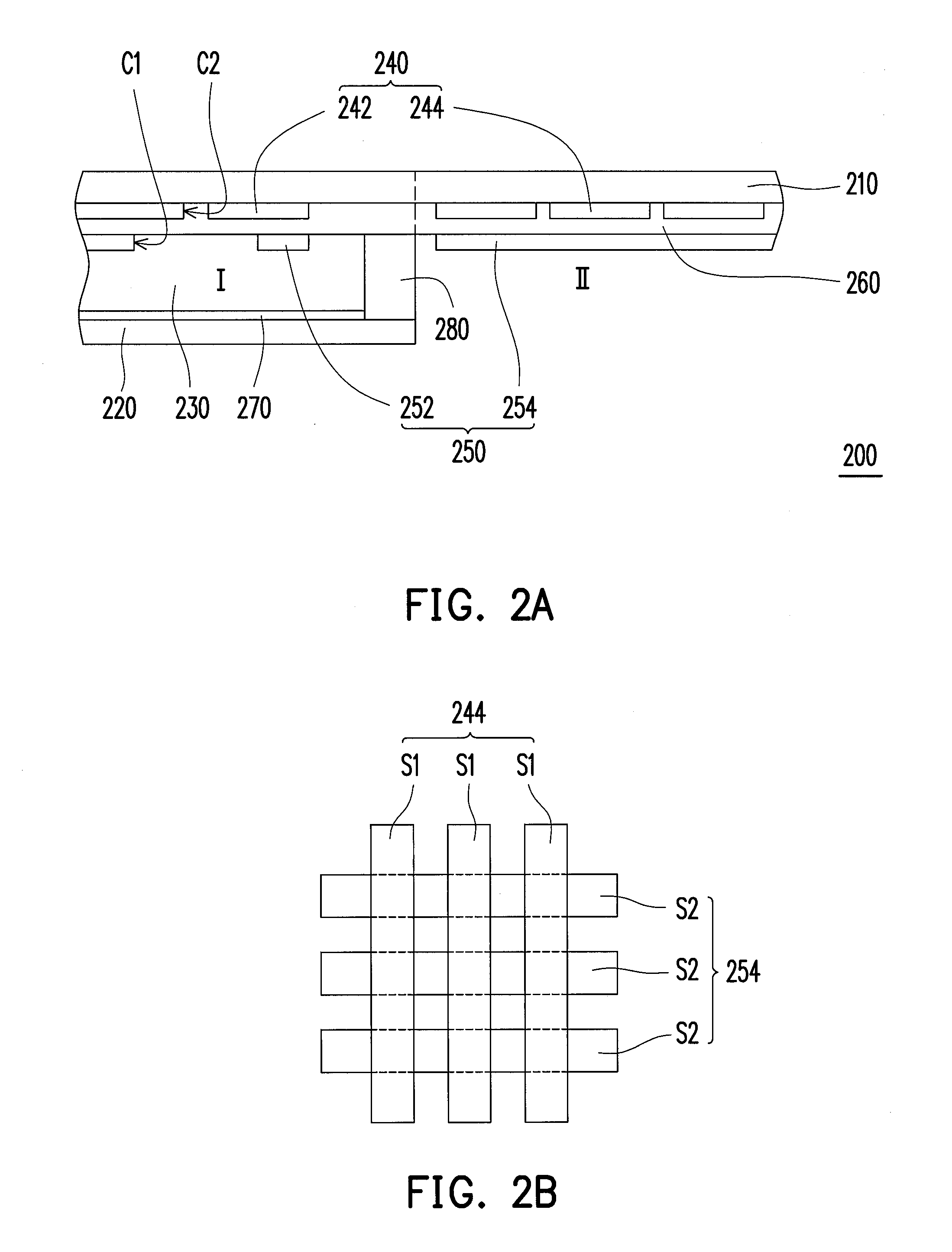
[0024]FIG. 2A is a schematic cross-sectional view of a touch display panel according to the invention. Referring to FIG. 2A, a touch display panel 200 includes a display area I for displaying an image and an operation area II for performing a touch operation. The touch display panel 200 includes a first substrate 210, a second substrate 220, a display medium 230, a first transparent electrode layer 240, a second transparent electrode layer 250, a dielectric layer 260, an active array device 270, and a sealant 280.
[0025]The second substrate 220 and the first substrate 210 are disposed opposite to each other. The display medium 230 is sandwiched between the first substrate 210 and the second substrate 220. The active array device 270 is disposed on the second substrate 220. The first transparent electrode layer 240 is disposed on the first substrate 210. Moreover, the dielectric layer 260 is disposed on the first transparent electrode layer 240. The second transparent electrode layer ...
third embodiment
[0033]FIG. 4A shows a schematic cross-sectional view of a touch display panel according to the invention, and FIG. 4B is a schematic top view of a touch device shown in FIG. 4A. Referring to FIGS. 4A and 4B simultaneously, a touch display panel 400 has a display area I and an operation area II located beside the display area I. The touch display panel 400 includes a first substrate 210, a second substrate 320, a display medium 230, a first transparent electrode layer 440, a second transparent electrode layer 450, a dielectric layer 260, and an active array device 270. The touch display panel 400 is different from the foregoing embodiments mainly in the pattern design of the first transparent electrode layer 440 and the second transparent electrode layer 450.
[0034]In details, the first transparent electrode layer 440 includes a first display area pattern 242 located in the display area I and a first operation area pattern 444 located in the operation area II. The second transparent e...
fourth embodiment
[0038]FIG. 5A shows a schematic cross-sectional view of a touch display panel according to the invention, and FIG. 5B is a schematic top view of a touch device shown in FIG. 5A. Referring to FIGS. 5A and 5B simultaneously, a touch display panel 500 also has a display area I and an operation area II located beside the display area I. The touch display panel 500 and the touch display panel 400 are mainly different in the design of the sensing series, so there is no more detailed description for the same devices herein.
[0039]In the present embodiment, a first operation area pattern 544 of a first transparent electrode layer 540 includes a plurality of first sensing pads P3, a plurality of second sensing pads P4, and a plurality of first connecting portions W3. The first sensing pads P3 and the second sensing pads P4 are arranged in a cross arrangement, and the first connecting portions W3 are configured for serially connecting the first sensing pads P3 to constitute a plurality of firs...
PUM
 Abstract
Description
Claims
Application Information